HT1647_05中文资料
HT1647
4-Level Gray Scale 64′16LCD Controller for I/O MCU
Rev.1.301November 10,2005
Features
·Operating voltage:2.7V~5.2V ·Built-in 32kHz RC oscillator
·External 32.768kHz crystal oscillator or 32kHz fre-quency source input
·Standby current:<1m A at 3V,<2m A at 5V
·Internal resistor type:1/5bias or 1/4bias,1/16duty ·Two selectable LCD frame frequencies:89Hz or
170Hz
·Max.64′16patterns,64segments and 16commons ·Built-in bit-map display RAM:2048bits (=64′16′2
bits)
·Built-in internal resistor type bias generator ·Six-wire interface (four data wires)·Eight kinds of time base/WDT selection ·Time base or WDT overflow output
·R/W address auto increment ·Built-in buzzer driver (2kHz/4kHz)
·Power down command reduces power consumption ·Software configuration feature
·Data mode and Command mode instructions ·Three data accessing modes
·Provides VLCD pin to adjust LCD operating voltage ·Provides three kinds of bias current programming ·Control of TN-type,STN-type LCDs and ECB-type
LCDs
·Four-level gray scale output for TN-type,STN-type
LCDs panel
·Four-color output for ECB-type LCDs panel ·100-pin QFP package and in chip form
General Description
HT1647is a peripheral device specially designed for I/O type MCU used to expand the display capability.The max.display segment of the device are 1024patterns (64segments and 16commons).It also supports four data bits interface,buzzer sound,Watchdog Timer or time base timer functions.The HT1647is a memory mapping and multi-function LCD controller.Since the HT1647can control ECB-type (Electrically Controlled Birefringence)LCDs in addition to current TN-type (Twisted Nematic)or STN-type (Super Twisted Ne-matic)LCDs,it can support 4-color display as well as
4-level gray scale display.It displays 4-level gray scale output when the HT1647drives a TN-type,STN-type LCDs.It displays four color output when the HT1647drives an ECB-type.HT1647uses PWM (Pulse Width Modulation)technique.The software configuration fea-ture of the HT1647make it suitable for multiple LCD ap-plications including LCD modules and display subsystems.Only six lines (CS,WR,DB0~DB3)are re-quired for the interface between the host controller and the HT1647.
Applications
·Leisure products ·Games
·Personal digital assistant
·Cellular phone
·Global positioning system ·Consumer
electronics
Technical Document
·FAQs
·Application Note
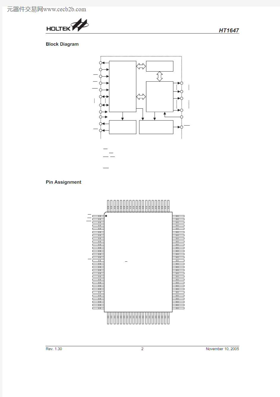
Block Diagram
Pin Assignment
Rev.1.302November10,2005
Pad Assignment
Chip size:3865′3770(m m)2
*The IC substrate should be connected to VSS in the PCB layout artwork.
Pad Coordinates Unit:m m Pad No.X Y Pad No.X Y Pad No.X Y
1-1774.501708.3034-331.40-1600.00671775.70795.30 2-1779.301409.8035-194.50-1558.30681775.70927.10 3-1779.301281.8036-48.00-1600.00691775.701055.10 4-1779.301150.003787.40-1600.00701775.701186.90 5-1779.301022.0038235.20-1600.00711775.701314.90 6-1779.30890.2039383.40-1600.00721775.701446.70 7-1779.30762.2040530.40-1600.00731775.701574.70 8-1779.30630.4041678.60-1600.00741775.701706.50 9-1779.30502.4042875.00-1712.30751471.101708.30 10-1779.30370.60431003.00-1712.30761343.101708.30 11-1779.30242.60441134.80-1712.30771211.301708.30 12-1779.30110.80451262.80-1712.30781083.301708.30 13-1779.30-17.20461394.60-1712.3079951.501708.30
Rev.1.303November10,2005
Pad No.X Y Pad No.X Y Pad No.X Y 14-1779.30-149.00471522.60-1712.3080823.501708.30 15-1779.30-277.00481654.40-1712.3081691.701708.30 16-1779.30-408.80491782.40-1712.3082563.701708.30 17-1779.30-536.80501775.70-1411.1083431.901708.30 18-1779.30-668.60511775.70-1283.1084303.901708.30 19-1779.30-796.60521775.70-1151.3085172.101708.30 20-1779.30-928.80531775.70-1023.308644.101708.30 21-1779.30-1056.80541775.70-891.5087-87.701708.30 22-1779.30-1189.00551775.70-763.5088-215.701708.30 23-1690.00-1375.40561775.70-631.7089-347.501708.30 24-1690.00-1515.40571775.70-503.7090-475.501708.30 25-1690.00-1651.00581775.70-371.9091-607.301708.30 26-1430.20-1599.90591775.70-243.9092-735.301708.30 27-1294.80-1599.90601775.70-112.1093-867.101708.30 28-1149.50-1599.90611775.7015.9094-995.101708.30 29-1013.90-1599.90621775.70147.7095-1126.901708.30 30-872.80-1600.00631775.70275.7096-1254.901708.30 31-738.30-1600.00641775.70407.5097-1386.701708.30 32-600.10-1600.00651775.70535.5098-1514.701708.30 33-465.60-1600.00661775.70667.3099-1646.501708.30
Pad Description
Pad No.Pad Name I/O Description
23CS I Chip selection input with pull-high resistor.When the CS is logic high,the data and command read from or write to the HT1647are disabled.The serial interface circuit is also reset.But if the CS is at a logic low level and is input to the CS pad,the data and command transmission between the host control-ler and the HT1647are all enabled.
24RD I READ clock input with pull-high resistor.Data in the RAM of the HT1647are clocked out on the rising edge of the RD signal.The clocked out data will ap-pear on the data line.The host controller can use the next falling edge to latch the clocked out data.
25WR I WRITE clock input with pull-high resistor.Data on the DATA line are latched into the HT1647on the rising edge of the WR signal.
26~29DB0~DB3I/O Parallel data input/output with a pull-high resistor
30VSS?Negative power supply for logic circuit,ground
31OSCI I The OSCI and OSCO pads are connected to a32.768kHz crystal in order to
generate a system clock.If the system clock comes from an external clock
source,the external clock source should be connected to the OSCI pad.But
if an on-chip RC oscillator is selected,the OSCI and OSCO pads can be left
open.
32OSCO O
33VDD?Positive power supply for logic circuit
34VLCD I Power supply for LCD driver circuit
35IRQ O Time base or Watchdog Timer overflow flag,NMOS open drain output.
36,37BZ,BZ O2kHz or4kHz frequency output pair(tristate output buffer)
38~41T1~T4I Not connected
42~57COM0~COM15O LCD common outputs
58~99,
1~22
SEG0~SEG63O LCD segment outputs
Rev.1.304November10,2005
Absolute Maximum Ratings
Supply Voltage...........................V SS-0.3V to V SS+5.5V Storage Temperature............................-50°C to125°C Input Voltage.............................V SS-0.3V to V DD+0.3V Operating Temperature...........................-25°C to75°C
Note:These are stress ratings only.Stresses exceeding the range specified under2Absolute Maximum Ratings2may cause substantial damage to the device.Functional operation of this device at other conditions beyond those listed in the specification is not implied and prolonged exposure to extreme conditions may affect device reliabil-ity.
D.C.Characteristics Ta=25°C
Symbol Parameter
Test Conditions
Min.Typ.Max.Unit V DD Conditions
V DD Operating Voltage?? 2.7? 5.2V
I DD1Operating Current 3V No load/LCD ON
On-chip RC oscillator
?150250m A 5V?250370m A
I DD2Operating Current 3V No load/LCD ON
Crystal oscillator
?135200m A 5V?200300m A
I DD11Operating Current 3V No load/LCD OFF
On-chip RC oscillator
?1530m A 5V?5070m A
I DD22Operating Current 3V No load/LCD OFF
Crystal oscillator
?210m A 5V?310m A
I STB Standby Current 3V
No load,Power down mode
??1m A 5V??2m A
V IL Input Low Voltage 3V
DB0~DB3,WR,CS,RD
0?0.6V 5V0? 1.0V
V IH Input High Voltage 3V
DB0~DB3,WR,CS,RD
2.4?3V 5V 4.0?5V
I OL1BZ,BZ,IRQ Sink Current 3V V OL=0.3V 1.2 2.5?mA 5V V OL=0.5V36?mA
I OH1BZ,BZ Source Current 3V V OH=2.7V-0.9-1.8?mA 5V V OH=4.5V-2-4?mA
I OL2DB0~DB3Sink Current 3V V OL=0.3V 1.2 2.5?mA 5V V OL=0.5V36?mA
I OH2DB0~DB3Source Current 3V V OH=2.7V-0.9-1.8?mA 5V V OH=4.5V-2-4?mA
I OL3LCD Common Sink Current 3V V OL=0.3V80160?m A 5V V OL=0.5V180360?m A
I OH3LCD Common Source Current 3V V OH=2.7V-40-80?m A 5V V OH=4.5V-90-180?m A
I OL4LCD Segment Sink Current 3V V OL=0.3V50100?m A 5V V OL=0.5V120240?m A
I OH4LCD Segment Source Current 3V V OH=2.7V-30-60?m A 5V V OH=4.5V-70-140?m A
R PH Pull-high Resistor 3V
DB0~DB3,WR,CS,RD
150250410k W 5V60125210k W
Rev.1.305November10,2005
A.C.Characteristics Ta=25°C
Symbol Parameter
Test Conditions
Min.Typ.Max.Unit V DD Conditions
f SYS1System Clock 3V
On-chip RC oscillator
223240kHz 5V243240kHz
f SYS2System Clock 3V
Crystal oscillator
?32.768?kHz 5V?32.768?kHz
f SYS3System Clock 3V
External clock source
?32?kHz 5V?32?kHz
f LCD1LCD Frame Frequency 3V
On-chip RC oscillator
61/11789/170111/213Hz 5V61/11789/170111/213Hz
f LCD2LCD Frame Frequency 3V
Crystal oscillator
?64?Hz 5V?64?Hz
f LCD3LCD Frame Frequency 3V
External clock source
?64?Hz 5V?64?Hz
t COM LCD Common Period?n:Number of COM?n/f LCD?sec
f CLK14-Bit Data Clock(WR Pin)3V
Duty cycle50%
??150kHz 5V??300kHz
f CLK24-Bit Data Clock(RD Pin)3V
Duty cycle50%
??75kHz 5V??150kHz
t CS 4-Bit Interface Reset Pulse Width
(Figure3)
?CS?250?ns
t CLK WR,RD Input Pulse Width(Figure1)3V
Write mode 3.34
??m s Read mode 6.67
5V
Write mode 1.67
??m s Read mode 3.34
t r,t f Rise/Fall Time Serial Data Clock
Width(Figure1)
3V
??120?ns
5V
t su Setup Time for DB to WR,RD Clock
Width(Figure2)
3V
??120?ns
5V
t h Hold Time for DB to WR,RD Clock
Width(Figure2)
3V
??120?ns
5V
t su1Setup Time for CS to WR,RD Clock
Width(Figure3)
3V
??100?ns
5V
t h1Hold Time for CS to WR,RD Clock
Width(Figure3)
3V
??100?ns
5V
Rev.1.306November10,2005
Figure
1Figure2
Figure3 Functional Description
System Oscillator
The HT1647system clock is used to generate the time base/Watchdog Timer(WDT)clock frequency,LCD driving clock,and tone frequency.The clock source may be from an on-chip RC oscillator(32kHz),a crystal oscillator(32.768kHz),or an external32kHz clock by the S/W setting.The configuration of the system oscilla-tor is as shown.After the SYS DIS command is exe-cuted,the system clock will stop and the LCD bias generator will turn off.That command is available only for the on-chip RC oscillator or for the crystal oscillator. Once the system clock stops,the LCD display will be-come blank,and the time base/WDT loses its function as well.
The LCD OFF command is used to turn the LCD bias generator off.After the LCD bias generator switches off by issuing the LCD OFF command,using the SYS DIS command reduces power consumption,thus serving as a system power down command.But if the external clock source is chosen as the system clock,using the SYS DIS command can neither turn the oscillator off nor carry out the power down mode.The crystal oscillator option can be applied to connect an external frequency source of32kHz to the OSCI pin.In this case,the sys-tem fails to enter the power down mode,similar to the case in the external32kHz clock source operation.At the initial system power on,the HT1647is at the SYS DIS state.
Display Memory-RAM Structure
The static display RAM is organized into512′4bits and stores the display data.The contents of the RAM are di-rectly mapped to the contents of the LCD driver.Data in the RAM can be accessed by the READ,WRITE and READ-MODIFY-WRITE commands.The following is a mapping from the RAM to the LCD patterns.
System Oscillator Configuration
Rev.1.307November10,2005
Display Memory-RAM Structure
Gray Scale Level Decision
HT1647uses PWM technique to provide4-level gray scale display.Two bits of RAM data code((D3,D2)or (D1,D0))decide one pixel level of LCDs,level1~level divided by4.Every level must be defined as one kind of gray scale by PWM data(namely B4~B0)previously.
RAM Data Code
(D3,D2)or(D1,D0)
Choice Gray Scale Level (1,1)Level1
(1,0)Level2
(0,1)Level3
(0,0)Level4
RAM Data Defined Gray Scale Level
Frame Frequency
HT1647provides two kinds of frame frequency option by command code;89Hz and170Hz respectively. FRAME89Hz provides89Hz frame frequency and ac-tive segment signal width can be divided into24sec-tions concurrently.FRAME170Hz provides170Hz frame frequency and active segment signal width can be divided into13sections concurrently.The24sections display a particularly gray scale more than the13sec-tions by PWM data.The default is FRAME89Hz.Gray Scale Display
If the user choose89Hz frame frequency,a max.of24 sections can be programmed to suit a satisfactory gray scale in every level.Similarly,if the user choose170Hz frame frequency,a max.of13sections can be pro-grammed to suit a satisfactory gray scale in every level. HT1647provides5-bit PWM data to control the length of the section.In other words,a max.Of24gray scales are generated by5-bit binary PWM data.At FRAME89Hz mode,the HT1647only provides a max.of24adjust-able gray scales although32is the expressed max. value by5bits binary code.When5bits binary code value is more than23,the PWM control circuit uniformly regards23.To increase PWM data indicates to increase the length of the active segment signal.The varied length of the active segment signal displays varied gray scale in TN-type,STN-type LCDs(refer to table1).Simi-larly,it displays varied color in ECB-type LCDs.The color display is derived from ECB-type LCD specifica-tion.At FRAME170Hz mode,the HT1647only provides a max.of13adjustable gray scales although32is the expressed max.value by5bits binary code.When the5 bits binary code value is more than12,the PWM control circuit uniformly regards12.The user must appoint four kinds of PWM data to four kinds of different gray scale level by commanding PWM data(refer to table2).
Name Command Code Function
FRAME170Hz X100-0001-1000-XXXX Select170Hz frame frequency and active segment signal width can be divided into13sections
FRAME89Hz X100-0001-1101-XXXX Select89Hz frame frequency and active segment signal width can be divided into24sections
Frame Frequency Selection Command Code
Rev.1.308November10,2005
Relationship Table between PWM Data and Gray Scale
Rev.1.309November 10,2005
Table 1:FRAME 89Hz Mode
Table 2:FRAME 170Hz Mode
Note:
The varied PWM data displays various gray scale in TN-type,STN-type LCDs.
The color display derives from ECB-type LCD ¢s specification.
Name Command Code
Function
GRS LEVEL 1X 100-001B4-B3B2B1B0-XXXX Set PWM data in gray scale level 1GRS LEVEL 2X 100-010B4-B3B2B1B0-XXXX Set PWM data in gray scale level 2GRS LEVEL 3
X 100-011B4-B3B2B1B0-XXXX Set PWM data in gray scale level 3GRS LEVEL 4
X 100-100B4-B3B2B1B0-XXXX
Set PWM data in gray scale level 4
Four Kinds of Gray Scale Level Command Code
Example of Waveform (B Type)in 1/5Bias,1/16Duty Cycle Drive
Time Base and Watchdog Timer-WDT
The time base generator and WDT share the same counter which is divided by256.The IRQ clock can be pro-grammed as1Hz,2Hz,....,128Hz output.TIMER DIS/EN/CLR,WDT DIS/EN/CLR and IRQ EN/DIS are in-dependent from each other.Once the WDT time-out oc-curs,the IRQ pin will remain at a logic low level until the CLR WDT or the IRQ DIS command is issued.
If an external clock is selected as the system frequency source,the SYS DIS command turns out invalid and the power down mode fails to be carried out until the exter-nal clock source is removed.
Buzzer Tone Output
A simple tone generator is implemented in the HT1647. The tone generator can output a pair of differential driv-ing signals on the BZ and BZ which are used to generate a single tone.
By executing the TONE4K and TONE2K commands there are two tone frequency outputs selectable that can turn on the tone output.The TONE4K and TONE2K commands set the tone frequency to4kHz and2kHz,re-spectively.The tone output can be turned off by invoking the TONE OFF command.The tone outputs,namely BZ and BZ,are a pair of differential driving outputs used to drive a piezo buzzer.Once the system is disabled or the tone output is inhibited,the BZ and the BZ outputs will remain at low https://www.360docs.net/doc/1211010135.html,mand Format
The HT1647can be configured by software setting. There are two mode commands to configure the HT1647resource and to transfer the LCD display data.
The configuration mode of the HT1647is called com-mand mode,and its command mode ID is100.The command mode consists of a system configuration command,a system frequency selection command,an LCD configuration command,a tone frequency selec-tion command,a bias current selection command,a gray scale level selection command,a timer/WDT set-ting command,and an operating command.The data mode,on the other hand,includes READ,WRITE,and READ-MODIFY-WRITE operations.
The following are the data mode ID and the command mode ID:
Operation Mode ID READ Data110 WRITE Data101 READ-MODIFY-WRITE Data101 COMMAND Command100
If successive commands have been issued,the com-mand mode ID can be omitted.While the system is op-erating in the non-successive command or the non-successive address data mode,the CS pin should be set to212and the previous operation mode will also be reset.The CS pin returns to202,so a new operation mode ID should be issued first.
Time Base and WDT Configurations
Name Command Code Function
TONE OFF X100-0000-1000-XXXX Turn-off tone output
TONE4K X100-0001-0000-XXXX Turn-on tone output,tone frequency is4kHz
TONE2K X100-0001-0001-XXXX Turn-on tone output,tone frequency is2kHz
Buzzer Tone Output Command Code
Rev.1.3010November10,2005
Bias Generator
The HT1647bias voltage belongs to internal resistor type.It provides two kinds of bias option named1/5bias and1/4bias respectively.It is recommended to select 1/5bias to fit TN-type,STN-type LCDs and select1/4 bias to fit ECB-type LCDs.It also provides three kinds of bias current option by programming to suitably drive an LCD panel.The three kinds of bias current are large,middle,and small,https://www.360docs.net/doc/1211010135.html,ually,large panel LCD can be excellently displayed by large bias current. Relatively,it consumes large current when LCD ON command is used.Small bias current provides low power consumption during On condition when the LCD is normally displayed.The following are the reference value table.
V LCD Bias Large Bias Current Middle Bias Current Small Bias Current 4V1/5300m A100m A40m A
4V1/4375m A125m A50m A
Internal Resistor Type Bias Generator Configurations
Interfacing
Only six lines are required to interface with the HT1647. The CS line is used to initialize the serial interface circuit and to terminate the communication between the host controller and the HT1647.If the CS pin is set to1,the data and command issued between the host controller and the HT1647are first disabled and then initialized. Before issuing a mode command or mode switching,a high level pulse is required to initialize the serial inter-face of the HT1647.The DB0~DB3are the4-bit parallel data input/output lines.Data to be read or written or commands to be written have to pass through the DB0~DB3lines.The RD line is the READ clock input. Data in the RAM are clocked out on the falling edge of the
signal,and the clocked out data will then appear on the DB0~DB3lines.It is recommended that the host controller read correct data during the interval between the rising edge and the next falling edge of the RD signal. The line is the WRITE clock input.The data,ad-dress,and command on the DB0~DB3lines are all clocked into the HT1647on the rising edge of the signal.There is an optional IRQ line to be used as an in-terface between the host controller and the HT1647. The IRQ pin can be selected as a timer output or a WDT overflow flag output by the S/W setting.The host con-troller can perform the time base or the WDT function by connecting with the pin of the HT1647.
Rev.1.3011November10,2005
Timing Diagrams
READ mode(command ID code:110)
WRITE mode(command ID code:101)
Rev.1.3012November10,2005
READ-MODIFY-WRITE mode(command ID code:101)
Command mode(command ID code:100)
Note:2X2stands for don¢t care
Rev.1.3013November10,2005
Application Circuits
Host Controller with an HT1647Display System
*Note:The connection of IRQ and RD pin can be selected depending on the MCU.
The voltage applied to V LCD pin must be lower than V DD.
Adjust VR to fit LCD display,at V DD=5V,V LCD=4V,VR=15k W±20%.
It is recommended to select1/5bias to fit TN-type,STN-type LCDs and select1/4bias to fit ECB-type LCDs.
Adjust R(external pull high resistance)to fit user¢s time base clock.
Instruction Set Summary
Name Command Code D/C Function Def. READ A8110-A7A6A5A4A3A2A1A0D3D2D1D0D Read data from the RAM
WRITE A8101-A7A6A5A4A3A2A1A0D3D2D1D0D Write data to the RAM
READ-MODIFY-
WRITE
A8101-A7A6A5A4A3A2A1A0D3D2D1D0D Read and Write data to the RAM
SYS DIS X100-0000-0000-XXXX C Turn Off both system oscillator and LCD bias generator
Yes
SYS EN X100-0000-0001-XXXX C Turn On system oscillator
LCD OFF X100-0000-0010-XXXX C Turn Off LCD display Yes LCD ON X100-0000-0011-XXXX C Turn On LCD display
TIMER DIS X100-0000-0100-XXXX C Disable time base output Yes WDT DIS X100-0000-0101-XXXX C Disable WDT time-out flag output Yes TIMER EN X100-0000-0110-XXXX C Enable time base output
WDT EN X100-0000-0111-XXXX C Enable WDT time-out flag output
TONE OFF X100-0000-1000-XXXX C Turn Off tone outputs Yes CLR TIMER X100-0000-1101-XXXX C Clear the contents of the time base generator CLR WDT X100-0000-1111-XXXX C Clear the contents of the WDT stage
TONE4K X100-0001-0000-XXXX C Turn on tone output,tone frequency output: 4kHz
TONE2K X100-0001-0001-XXXX C Turn on tone output,tone frequency output: 2kHz
Rev.1.3014November10,2005
Name Command Code D/C Function Def. IRQ DIS X100-0001-0010-XXXX C Disable IRQ output Yes IRQ EN X100-0001-0011-XXXX C Enable IRQ output
RC32K X100-0001-0100-XXXX C System clock source,on-chip RC oscillator Yes
EXT(XTAL)X100-0001-0101-XXXX C System clock source,external32kHz clock source or crystal oscillator32.768kHz
LARGE BIAS X100-0001-0110-XXXX C Large bias current option Yes MIDDLE BIAS X100-0001-0111-XXXX C Middle bias current option
SMALL BIAS X100-0001-1000-XXXX C Small bias current option
BIAS1/5X100-0001-1001-XXXX C LCD1/5bias option Yes BIAS1/4X100-0001-1010-XXXX C LCD1/4bias option
FRAME170Hz X100-0001-1100-XXXX C Selects170Hz frame frequency and active segment signal width can be divided into13 sections
FRAME89Hz X100-0001-1101-XXXX C Selects89Hz frame frequency and active segment signal width can be divided into24 sections
Yes
GRS LEVEL1X100-001B4-B3B2B1B0-XXXX C Sets PWM data in gray scale level1 GRS LEVEL2X100-010B4-B3B2B1B0-XXXX C Sets PWM data in gray scale level2 GRS LEVEL3X100-011B4-B3B2B1B0-XXXX C Sets PWM data in gray scale level3 GRS LEVEL4X100-100B4-B3B2B1B0-XXXX C Sets PWM data in gray scale level4
F1X100-1010-0000-XXXX C Time base clock output:1Hz The WDT time-out flag after:4s
F2X100-1010-0001-XXXX C Time base clock output:2Hz The WDT time-out flag after:2s
F4X100-1010-0010-XXXX C Time base clock output:4Hz The WDT time-out flag after:1s
F8X100-1010-0011-XXXX C Time base clock output:8Hz
The WDT time-out flag after:1/2s
F16X100-1010-0100-XXXX C Time base clock output:16Hz The WDT time-out flag after:1/4s
F32X100-1010-0101-XXXX C Time base clock output:32Hz The WDT time-out flag after:1/8s
F64X100-1010-0110-XXXX C Time base clock output:64Hz
The WDT time-out flag after:1/16s
F128X100-1010-0111-XXXX C Time base clock output:128Hz
The WDT time-out flag after:1/32s
Yes
TEST X100-1111-1111-XXXX C Test mode,user don¢t use.
NORMAL X100-1111-1110-XXXX C Normal mode Yes Note:2X2stands for don¢t care
A8~A0:RAM address
D3~D0:RAM data
B4~B0:PWM data
D/C:Data/Command mode
Def.:Power-on reset default
All the bold forms,namely110,101,and100,are mode commands.Of these,100indicates the command mode ID.If successive commands have been issued,the command mode ID except for the first command will be omitted.The tone frequency source and the time base/WDT clock frequency source can be derived from an on-chip32kHz RC oscillator,a32.768kHz crystal oscillator,or an external32kHz clock.Calculation of the fre-quency is based on the system frequency sources as stated above.It is recommended that the host controller should initialize the HT1647after power-on reset,otherwise,power on reset may fail,which in turn leads to the malfunctioning of the HT1647.
Rev.1.3015November10,2005
Package Information
100-pin QFP(14′20)outline dimensions
Symbol
Dimensions in mm
Min.Nom.Max.
A18.80?19.20
B13.90?14.10
C24.80?25.20
D19.90?20.10
E?0.65?
F?0.30?
G 2.50? 3.10
H?? 3.40
I?0.10?
J1? 1.40
K0.10?0.20
a0°?7°
Rev.1.3016November10,2005
Holtek Semiconductor Inc.(Headquarters)
No.3,Creation Rd.II,Science Park,Hsinchu,Taiwan
Tel:886-3-563-1999
Fax:886-3-563-1189
https://www.360docs.net/doc/1211010135.html,
Holtek Semiconductor Inc.(Taipei Sales Office)
4F-2,No.3-2,YuanQu St.,Nankang Software Park,Taipei115,Taiwan
Tel:886-2-2655-7070
Fax:886-2-2655-7373
Fax:886-2-2655-7383(International sales hotline)
Holtek Semiconductor Inc.(Shanghai Sales Office)
7th Floor,Building2,No.889,Yi Shan Rd.,Shanghai,China200233
Tel:021-6485-5560
Fax:021-6485-0313
https://www.360docs.net/doc/1211010135.html,
Holtek Semiconductor Inc.(Shenzhen Sales Office)
5/F,Unit A,Productivity Building,Cross of Science M3rd Road and Gaoxin M2nd Road,Science Park,Nanshan District, Shenzhen,China518057
Tel:0755-8616-9908,8616-9308
Fax:0755-8616-9533
Holtek Semiconductor Inc.(Beijing Sales Office)
Suite1721,Jinyu Tower,A129West Xuan Wu Men Street,Xicheng District,Beijing,China100031
Tel:010-6641-0030,6641-7751,6641-7752
Fax:010-6641-0125
Holtek Semiconductor Inc.(Chengdu Sales Office)
709,Building3,Champagne Plaza,No.97Dongda Street,Chengdu,Sichuan,China610016
Tel:028-6653-6590
Fax:028-6653-6591
Holmate Semiconductor,Inc.(North America Sales Office)
46729Fremont Blvd.,Fremont,CA94538
Tel:510-252-9880
Fax:510-252-9885
https://www.360docs.net/doc/1211010135.html,
Copyrightó2005by HOLTEK SEMICONDUCTOR INC.
The information appearing in this Data Sheet is believed to be accurate at the time of publication.However,Holtek as-sumes no responsibility arising from the use of the specifications described.The applications mentioned herein are used solely for the purpose of illustration and Holtek makes no warranty or representation that such applications will be suitable without further modification,nor recommends the use of its products for application that may present a risk to human life due to malfunction or otherwise.Holtek¢s products are not authorized for use as critical components in life support devices or systems.Holtek reserves the right to alter its products without prior notification.For the most up-to-date information, please visit our web site at https://www.360docs.net/doc/1211010135.html,.
Rev.1.3017November10,2005