LSM303D
This is preliminary information on a new product now in development or undergoing evaluation. Details are subject to change without notice.
June 2012Doc ID 023312 Rev 1
1/54
LSM303D
Ultra compact high performance e-Compass 3D accelerometer and 3D magnetometer module
Datasheet — preliminary data
Features
■ 3 magnetic field channels and 3 acceleration channels
■±2/±4/±8/±12 gauss dynamically selectable magnetic full-scale
■±2/±4/±6/±8/±16 g dynamically selectable linear acceleration full-scale ■16-bit data output ■SPI / I 2C serial interfaces
■Analog supply voltage 2.16 V to 3.6 V ■Power-down mode / low-power mode ■
Programmable interrupt generators for free-fall, motion detection and magnetic field detection
■Embedded temperature sensor ■Embedded FIFO
■
ECOPACK ?, RoHS and “Green” compliant
Applications
■Tilt compensated compass ■Map rotation ■Position detection ■Motion activated functions ■Free-fall detection
■Click/double click recognition ■Pedometer
■Intelligent power saving for handheld devices ■Display orientation
■Gaming and virtual reality input devices ■Impact recognition and logging ■
Vibration monitoring and compensation
Description
The LSM303D is a system-in-package featuring a 3D digital linear acceleration sensor and a 3D digital magnetic sensor.
The LSM303D has linear acceleration full-scales of ±2g / ±4g / ±6g / ±8g / ±16g and a magnetic field full-scale of ±2 / ±4 / ±8 / ±12 gauss . All full-scales available are fully selectable by the user.The LSM303D includes an I 2C serial bus interface that supports standard and fast mode 100 kHz and 400 kHz and SPI serial standard interface.The system can be configured to generate an interrupt signal for free-fall, motion detection and magnetic field detection. Thresholds and timing of interrupt generators are programmable by the end user on the fly.
Magnetic and accelerometer parts can be
enabled or put into power-down mode separately.The LSM303D is available in plastic land grid array package (LGA) and is guaranteed to
operate over an extended temperature range from -40 °C to +85 °C. Table 1.
Device summary
Part number Temperature
range [°C]Package Packaging
LSM303D -40 to +85LGA-16Tray LSM303DTR
-40 to +85
LGA-16
Tape and reel
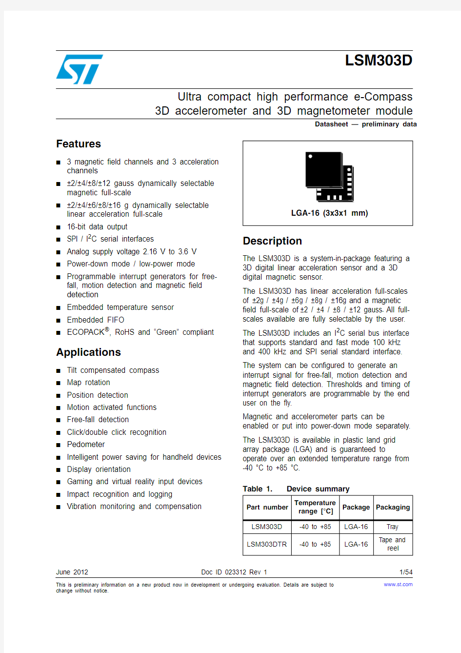
LGA-16 (3x3x1 mm)
https://www.360docs.net/doc/1f12458418.html,
Contents LSM303D
Contents
1Block diagram and pin description . . . . . . . . . . . . . . . . . . . . . . . . . . . . . 8
1.1Block diagram . . . . . . . . . . . . . . . . . . . . . . . . . . . . . . . . . . . . . . . . . . . . . . . 8
1.2Pin description . . . . . . . . . . . . . . . . . . . . . . . . . . . . . . . . . . . . . . . . . . . . . . 8
2Module specifications . . . . . . . . . . . . . . . . . . . . . . . . . . . . . . . . . . . . . . . 10
2.1Sensor characteristics . . . . . . . . . . . . . . . . . . . . . . . . . . . . . . . . . . . . . . . 10
2.2T emperature sensor characteristics . . . . . . . . . . . . . . . . . . . . . . . . . . . . . 11
2.3Electrical characteristics . . . . . . . . . . . . . . . . . . . . . . . . . . . . . . . . . . . . . . 12
2.4Communication interface characteristics . . . . . . . . . . . . . . . . . . . . . . . . . 13
2.4.1SPI - serial peripheral interface . . . . . . . . . . . . . . . . . . . . . . . . . . . . . . . 13
2.4.2Sensor I2C - inter IC control interface . . . . . . . . . . . . . . . . . . . . . . . . . . 14
2.5Absolute maximum ratings . . . . . . . . . . . . . . . . . . . . . . . . . . . . . . . . . . . . 15
3Terminology . . . . . . . . . . . . . . . . . . . . . . . . . . . . . . . . . . . . . . . . . . . . . . . 16
3.1Set/reset pulse . . . . . . . . . . . . . . . . . . . . . . . . . . . . . . . . . . . . . . . . . . . . . 16
3.2Sensitivity . . . . . . . . . . . . . . . . . . . . . . . . . . . . . . . . . . . . . . . . . . . . . . . . . 16
3.2.1Linear acceleration sensor sensitivity . . . . . . . . . . . . . . . . . . . . . . . . . . 16
3.2.2Magnetic sensor sensitivity . . . . . . . . . . . . . . . . . . . . . . . . . . . . . . . . . . 16
3.3Zero-g level . . . . . . . . . . . . . . . . . . . . . . . . . . . . . . . . . . . . . . . . . . . . . . . . 16
3.4Zero-gauss level . . . . . . . . . . . . . . . . . . . . . . . . . . . . . . . . . . . . . . . . . . . . 16
4Functionality . . . . . . . . . . . . . . . . . . . . . . . . . . . . . . . . . . . . . . . . . . . . . . 17
4.1Self-test . . . . . . . . . . . . . . . . . . . . . . . . . . . . . . . . . . . . . . . . . . . . . . . . . . 17
4.2T emperature sensor . . . . . . . . . . . . . . . . . . . . . . . . . . . . . . . . . . . . . . . . . 17
4.3FIFO . . . . . . . . . . . . . . . . . . . . . . . . . . . . . . . . . . . . . . . . . . . . . . . . . . . . . 17
4.4Factory calibration . . . . . . . . . . . . . . . . . . . . . . . . . . . . . . . . . . . . . . . . . . 18
5Application hints . . . . . . . . . . . . . . . . . . . . . . . . . . . . . . . . . . . . . . . . . . . 19
5.1External capacitors . . . . . . . . . . . . . . . . . . . . . . . . . . . . . . . . . . . . . . . . . . 19
5.2Pull-up resistors . . . . . . . . . . . . . . . . . . . . . . . . . . . . . . . . . . . . . . . . . . . . 19
5.3Digital Interface power supply . . . . . . . . . . . . . . . . . . . . . . . . . . . . . . . . . 20
5.4Soldering information . . . . . . . . . . . . . . . . . . . . . . . . . . . . . . . . . . . . . . . . 20 2/54Doc ID 023312 Rev 1
LSM303D Contents
5.5High-current wiring effects . . . . . . . . . . . . . . . . . . . . . . . . . . . . . . . . . . . . 20
6Digital interfaces . . . . . . . . . . . . . . . . . . . . . . . . . . . . . . . . . . . . . . . . . . . 21
6.1I2C serial interface . . . . . . . . . . . . . . . . . . . . . . . . . . . . . . . . . . . . . . . . . . 21
6.1.1I2C operation . . . . . . . . . . . . . . . . . . . . . . . . . . . . . . . . . . . . . . . . . . . . . 22
6.2SPI bus interface . . . . . . . . . . . . . . . . . . . . . . . . . . . . . . . . . . . . . . . . . . . 23
6.2.1SPI read . . . . . . . . . . . . . . . . . . . . . . . . . . . . . . . . . . . . . . . . . . . . . . . . . 25
6.2.2SPI write . . . . . . . . . . . . . . . . . . . . . . . . . . . . . . . . . . . . . . . . . . . . . . . . 26
6.2.3SPI read in 3-wire mode . . . . . . . . . . . . . . . . . . . . . . . . . . . . . . . . . . . . 26 7Output register mapping . . . . . . . . . . . . . . . . . . . . . . . . . . . . . . . . . . . . 28
8Register description . . . . . . . . . . . . . . . . . . . . . . . . . . . . . . . . . . . . . . . . 31
8.1TEMP_OUT_L (05h), TEMP_OUT_H (06h) . . . . . . . . . . . . . . . . . . . . . . . 31
8.2STATUS_M (07h) . . . . . . . . . . . . . . . . . . . . . . . . . . . . . . . . . . . . . . . . . . . 31
8.3OUT_X_L_M (08h), OUT_X_H_M (09h) . . . . . . . . . . . . . . . . . . . . . . . . . 32
8.4OUT_Y_L_M (0Ah), OUT_X_H_M (0Bh) . . . . . . . . . . . . . . . . . . . . . . . . . 32
8.5OUT_X_L_M (0Ch), OUT_X_H_M (0Dh) . . . . . . . . . . . . . . . . . . . . . . . . . 32
8.6WHO_AM_I (0Fh) . . . . . . . . . . . . . . . . . . . . . . . . . . . . . . . . . . . . . . . . . . . 32
8.7INT_CTRL_M (12h) . . . . . . . . . . . . . . . . . . . . . . . . . . . . . . . . . . . . . . . . . 32
8.8INT_SRC_M (13h) . . . . . . . . . . . . . . . . . . . . . . . . . . . . . . . . . . . . . . . . . . 33
8.9INT_THS_L_M (14h), INT_THS_H_M (15h) . . . . . . . . . . . . . . . . . . . . . . 33
8.10OFFSET_X_L_M (16h), OFFSET_X_H_M (17h) . . . . . . . . . . . . . . . . . . . 34
8.11OFFSET_Y_L_M (18h), OFFSET_Y_H_M (19h) . . . . . . . . . . . . . . . . . . . 34
8.12OFFSET_Z_L_M (1Ah), OFFSET_Z_H_M (1Bh) . . . . . . . . . . . . . . . . . . 34
8.13REFERENCE_X (1Ch) . . . . . . . . . . . . . . . . . . . . . . . . . . . . . . . . . . . . . . . 35
8.14REFERENCE_Y (1Dh) . . . . . . . . . . . . . . . . . . . . . . . . . . . . . . . . . . . . . . . 35
8.15REFERENCE_Z (1Eh) . . . . . . . . . . . . . . . . . . . . . . . . . . . . . . . . . . . . . . . 35
8.16CTRL0 (1Fh) . . . . . . . . . . . . . . . . . . . . . . . . . . . . . . . . . . . . . . . . . . . . . . 35
8.17CTRL1 (20h) . . . . . . . . . . . . . . . . . . . . . . . . . . . . . . . . . . . . . . . . . . . . . . . 35
8.18CTRL2 (21h) . . . . . . . . . . . . . . . . . . . . . . . . . . . . . . . . . . . . . . . . . . . . . . . 36
8.19CTRL3 (22h) . . . . . . . . . . . . . . . . . . . . . . . . . . . . . . . . . . . . . . . . . . . . . . . 37
8.20CTRL4 (23h) . . . . . . . . . . . . . . . . . . . . . . . . . . . . . . . . . . . . . . . . . . . . . . . 38
8.21CTRL5 (24h) . . . . . . . . . . . . . . . . . . . . . . . . . . . . . . . . . . . . . . . . . . . . . . . 39
Doc ID 023312 Rev 13/54
Contents LSM303D
8.22CTRL6 (25h) . . . . . . . . . . . . . . . . . . . . . . . . . . . . . . . . . . . . . . . . . . . . . . . 39
8.23CTRL7 (26h) . . . . . . . . . . . . . . . . . . . . . . . . . . . . . . . . . . . . . . . . . . . . . . . 40
8.24STATUS_A (27h) . . . . . . . . . . . . . . . . . . . . . . . . . . . . . . . . . . . . . . . . . . . 41
8.25OUT_X_L_A (28h), OUT_X_H_A (29h) . . . . . . . . . . . . . . . . . . . . . . . . . . 42
8.26OUT_Y_L_A (2Ah), OUT_X_H_A (2Bh) . . . . . . . . . . . . . . . . . . . . . . . . . 42
8.27OUT_X_L_A (2Ch), OUT_X_H_A (2Dh) . . . . . . . . . . . . . . . . . . . . . . . . . 42
8.28FIFO_CTRL (2Eh) . . . . . . . . . . . . . . . . . . . . . . . . . . . . . . . . . . . . . . . . . . 42
8.29FIFO_SRC (2Fh) . . . . . . . . . . . . . . . . . . . . . . . . . . . . . . . . . . . . . . . . . . . 42
8.30IG_CFG1 (30h) . . . . . . . . . . . . . . . . . . . . . . . . . . . . . . . . . . . . . . . . . . . . . 43
8.31IG_SRC1 (31h) . . . . . . . . . . . . . . . . . . . . . . . . . . . . . . . . . . . . . . . . . . . . . 44
8.32IG_THS1 (32h) . . . . . . . . . . . . . . . . . . . . . . . . . . . . . . . . . . . . . . . . . . . . . 45
8.33IG_DUR1 (33h) . . . . . . . . . . . . . . . . . . . . . . . . . . . . . . . . . . . . . . . . . . . . 45
8.34IG_CFG2 (34h) . . . . . . . . . . . . . . . . . . . . . . . . . . . . . . . . . . . . . . . . . . . . . 45
8.35IG_SRC2 (35h) . . . . . . . . . . . . . . . . . . . . . . . . . . . . . . . . . . . . . . . . . . . . . 46
8.36IG_THS2 (36h) . . . . . . . . . . . . . . . . . . . . . . . . . . . . . . . . . . . . . . . . . . . . . 47
8.37IG_DUR2 (37h) . . . . . . . . . . . . . . . . . . . . . . . . . . . . . . . . . . . . . . . . . . . . 47
8.38CLICK_CFG (38h) . . . . . . . . . . . . . . . . . . . . . . . . . . . . . . . . . . . . . . . . . . 47
8.39CLICK_SRC (39h) . . . . . . . . . . . . . . . . . . . . . . . . . . . . . . . . . . . . . . . . . . 48
8.40CLICK_THS (3Ah) . . . . . . . . . . . . . . . . . . . . . . . . . . . . . . . . . . . . . . . . . . 49
8.41TIME_LIMIT (3Bh) . . . . . . . . . . . . . . . . . . . . . . . . . . . . . . . . . . . . . . . . . . 49
8.42TIME_LATENCY (3Ch) . . . . . . . . . . . . . . . . . . . . . . . . . . . . . . . . . . . . . . . 49
8.43TIME WINDOW (3Dh) . . . . . . . . . . . . . . . . . . . . . . . . . . . . . . . . . . . . . . . 49
8.44Act_THS (3Eh) . . . . . . . . . . . . . . . . . . . . . . . . . . . . . . . . . . . . . . . . . . . . . 50
8.45Act_DUR (3Fh) . . . . . . . . . . . . . . . . . . . . . . . . . . . . . . . . . . . . . . . . . . . . . 50 9Package Information . . . . . . . . . . . . . . . . . . . . . . . . . . . . . . . . . . . . . . . . 51 10Revision history . . . . . . . . . . . . . . . . . . . . . . . . . . . . . . . . . . . . . . . . . . . 53
4/54Doc ID 023312 Rev 1
LSM303D List of tables List of tables
Table 1.Device summary. . . . . . . . . . . . . . . . . . . . . . . . . . . . . . . . . . . . . . . . . . . . . . . . . . . . . . . . . . 1 Table 2.Pin description . . . . . . . . . . . . . . . . . . . . . . . . . . . . . . . . . . . . . . . . . . . . . . . . . . . . . . . . . . . 9 Table 3.Sensor characteristics . . . . . . . . . . . . . . . . . . . . . . . . . . . . . . . . . . . . . . . . . . . . . . . . . . . . 10 Table 4.Temperature sensor characteristics. . . . . . . . . . . . . . . . . . . . . . . . . . . . . . . . . . . . . . . . . . 11 Table 5.Electrical characteristics. . . . . . . . . . . . . . . . . . . . . . . . . . . . . . . . . . . . . . . . . . . . . . . . . . . 12 Table 6.SPI slave timing values. . . . . . . . . . . . . . . . . . . . . . . . . . . . . . . . . . . . . . . . . . . . . . . . . . . . 13 Table 7.I2C slave timing values. . . . . . . . . . . . . . . . . . . . . . . . . . . . . . . . . . . . . . . . . . . . . . . . . . . . 14 Table 8.Absolute maximum ratings. . . . . . . . . . . . . . . . . . . . . . . . . . . . . . . . . . . . . . . . . . . . . . . . . 15 Table 9.Serial interface pin description . . . . . . . . . . . . . . . . . . . . . . . . . . . . . . . . . . . . . . . . . . . . . . 21 Table 10.I2C terminology. . . . . . . . . . . . . . . . . . . . . . . . . . . . . . . . . . . . . . . . . . . . . . . . . . . . . . . . . . 21 Table 11.SAD+read/write patterns. . . . . . . . . . . . . . . . . . . . . . . . . . . . . . . . . . . . . . . . . . . . . . . . . . . 22 Table 12.Transfer when master is writing one byte to slave . . . . . . . . . . . . . . . . . . . . . . . . . . . . . . . 22 Table 13.Transfer when master is writing multiple bytes to slave . . . . . . . . . . . . . . . . . . . . . . . . . . . 23 Table 14.Transfer when master is receiving (reading) one byte of data from slave . . . . . . . . . . . . . 23 Table 15.Transfer when master is receiving (reading) multiple bytes of data from slave . . . . . . . . . 23 Table 16.Register address map. . . . . . . . . . . . . . . . . . . . . . . . . . . . . . . . . . . . . . . . . . . . . . . . . . . . . 28 Table 17.STATUS_M register . . . . . . . . . . . . . . . . . . . . . . . . . . . . . . . . . . . . . . . . . . . . . . . . . . . . . . 31 Table 18.STATUS_M description . . . . . . . . . . . . . . . . . . . . . . . . . . . . . . . . . . . . . . . . . . . . . . . . . . . 31 Table 19.WHO_AM_I register . . . . . . . . . . . . . . . . . . . . . . . . . . . . . . . . . . . . . . . . . . . . . . . . . . . . . . 32 Table 20.INT_CTRL_M register. . . . . . . . . . . . . . . . . . . . . . . . . . . . . . . . . . . . . . . . . . . . . . . . . . . . . 32 Table 21.INT_CTRL_M description. . . . . . . . . . . . . . . . . . . . . . . . . . . . . . . . . . . . . . . . . . . . . . . . . . 32 Table 22.INT_SRC_M register . . . . . . . . . . . . . . . . . . . . . . . . . . . . . . . . . . . . . . . . . . . . . . . . . . . . . 33 Table 23.INT_SRC_M description. . . . . . . . . . . . . . . . . . . . . . . . . . . . . . . . . . . . . . . . . . . . . . . . . . . 33 Table 24.INT_THS_L_M . . . . . . . . . . . . . . . . . . . . . . . . . . . . . . . . . . . . . . . . . . . . . . . . . . . . . . . . . . 33 Table 25.INT_THS_H_M. . . . . . . . . . . . . . . . . . . . . . . . . . . . . . . . . . . . . . . . . . . . . . . . . . . . . . . . . . 34 Table 26.OFFSET_X_L_M . . . . . . . . . . . . . . . . . . . . . . . . . . . . . . . . . . . . . . . . . . . . . . . . . . . . . . . . 34 Table 27.OFFSET_X_H_M . . . . . . . . . . . . . . . . . . . . . . . . . . . . . . . . . . . . . . . . . . . . . . . . . . . . . . . . 34 Table 28.OFFSET_Y_L_M . . . . . . . . . . . . . . . . . . . . . . . . . . . . . . . . . . . . . . . . . . . . . . . . . . . . . . . . 34 Table 29.OFFSET_Y_H_M . . . . . . . . . . . . . . . . . . . . . . . . . . . . . . . . . . . . . . . . . . . . . . . . . . . . . . . . 34 Table 30.OFFSET_Z_L_M . . . . . . . . . . . . . . . . . . . . . . . . . . . . . . . . . . . . . . . . . . . . . . . . . . . . . . . . 34 Table 31.OFFSET_Z_H_M . . . . . . . . . . . . . . . . . . . . . . . . . . . . . . . . . . . . . . . . . . . . . . . . . . . . . . . . 34 Table 32.CTRL0 register. . . . . . . . . . . . . . . . . . . . . . . . . . . . . . . . . . . . . . . . . . . . . . . . . . . . . . . . . . 35 Table 33.CTRL0 description . . . . . . . . . . . . . . . . . . . . . . . . . . . . . . . . . . . . . . . . . . . . . . . . . . . . . . . 35 Table 34.CTRL1 register. . . . . . . . . . . . . . . . . . . . . . . . . . . . . . . . . . . . . . . . . . . . . . . . . . . . . . . . . . 35 Table 35.CTRL1 description . . . . . . . . . . . . . . . . . . . . . . . . . . . . . . . . . . . . . . . . . . . . . . . . . . . . . . . 36 Table 36.Acceleration data rate configuration. . . . . . . . . . . . . . . . . . . . . . . . . . . . . . . . . . . . . . . . . . 36 Table 37.CTRL2 register. . . . . . . . . . . . . . . . . . . . . . . . . . . . . . . . . . . . . . . . . . . . . . . . . . . . . . . . . . 36 Table 38.CTRL2 register description. . . . . . . . . . . . . . . . . . . . . . . . . . . . . . . . . . . . . . . . . . . . . . . . . 37 Table 39.Acceleration anti-alias filter bandwidth. . . . . . . . . . . . . . . . . . . . . . . . . . . . . . . . . . . . . . . . 37 Table 40.Acceleration full-scale selection . . . . . . . . . . . . . . . . . . . . . . . . . . . . . . . . . . . . . . . . . . . . . 37 Table 41.CTRL3 register. . . . . . . . . . . . . . . . . . . . . . . . . . . . . . . . . . . . . . . . . . . . . . . . . . . . . . . . . . 37 Table 42.CTRL3 register description. . . . . . . . . . . . . . . . . . . . . . . . . . . . . . . . . . . . . . . . . . . . . . . . . 37 Table 43.CTRL4 register. . . . . . . . . . . . . . . . . . . . . . . . . . . . . . . . . . . . . . . . . . . . . . . . . . . . . . . . . . 38 Table 44.CTRL4 register description. . . . . . . . . . . . . . . . . . . . . . . . . . . . . . . . . . . . . . . . . . . . . . . . . 38 Table 45.CTRL5 register. . . . . . . . . . . . . . . . . . . . . . . . . . . . . . . . . . . . . . . . . . . . . . . . . . . . . . . . . . 39 Table 46.CTRL5 register description. . . . . . . . . . . . . . . . . . . . . . . . . . . . . . . . . . . . . . . . . . . . . . . . . 39 Table 47.Magnetic data rate configuration . . . . . . . . . . . . . . . . . . . . . . . . . . . . . . . . . . . . . . . . . . . . 39 Table 48.CTRL6 register. . . . . . . . . . . . . . . . . . . . . . . . . . . . . . . . . . . . . . . . . . . . . . . . . . . . . . . . . . 39
Doc ID 023312 Rev 15/54
List of tables LSM303D Table 49.CTRL6 register description. . . . . . . . . . . . . . . . . . . . . . . . . . . . . . . . . . . . . . . . . . . . . . . . . 40 Table 50.Magnetic full-scale selection. . . . . . . . . . . . . . . . . . . . . . . . . . . . . . . . . . . . . . . . . . . . . . . . 40 Table 51.CTRL7 register. . . . . . . . . . . . . . . . . . . . . . . . . . . . . . . . . . . . . . . . . . . . . . . . . . . . . . . . . . 40 Table 52.CTRL7 register description. . . . . . . . . . . . . . . . . . . . . . . . . . . . . . . . . . . . . . . . . . . . . . . . . 40 Table 53.High-pass filter mode selection. . . . . . . . . . . . . . . . . . . . . . . . . . . . . . . . . . . . . . . . . . . . . . 40 Table 54.Magnetic sensor mode selection . . . . . . . . . . . . . . . . . . . . . . . . . . . . . . . . . . . . . . . . . . . . 41 Table 55.STATUS_A register . . . . . . . . . . . . . . . . . . . . . . . . . . . . . . . . . . . . . . . . . . . . . . . . . . . . . . 41 Table 56.STATUS_A description. . . . . . . . . . . . . . . . . . . . . . . . . . . . . . . . . . . . . . . . . . . . . . . . . . . . 41 Table 57.FIFO_CTRL register. . . . . . . . . . . . . . . . . . . . . . . . . . . . . . . . . . . . . . . . . . . . . . . . . . . . . . 42 Table 58.FIFO_CTRL register description. . . . . . . . . . . . . . . . . . . . . . . . . . . . . . . . . . . . . . . . . . . . . 42 Table 59.FIFO mode configuration . . . . . . . . . . . . . . . . . . . . . . . . . . . . . . . . . . . . . . . . . . . . . . . . . . 42 Table 60.FIFO_SRC register. . . . . . . . . . . . . . . . . . . . . . . . . . . . . . . . . . . . . . . . . . . . . . . . . . . . . . . 42 Table 61.FIFO_SRC description . . . . . . . . . . . . . . . . . . . . . . . . . . . . . . . . . . . . . . . . . . . . . . . . . . . . 43 Table 62.IG_CFG1 register. . . . . . . . . . . . . . . . . . . . . . . . . . . . . . . . . . . . . . . . . . . . . . . . . . . . . . . . 43 Table 63.IG_CFG1 register description. . . . . . . . . . . . . . . . . . . . . . . . . . . . . . . . . . . . . . . . . . . . . . . 43 Table 64.Interrupt mode . . . . . . . . . . . . . . . . . . . . . . . . . . . . . . . . . . . . . . . . . . . . . . . . . . . . . . . . . . 44 Table 65.IG_SRC1 register. . . . . . . . . . . . . . . . . . . . . . . . . . . . . . . . . . . . . . . . . . . . . . . . . . . . . . . . 44 Table 66.IG_SRC1 register description. . . . . . . . . . . . . . . . . . . . . . . . . . . . . . . . . . . . . . . . . . . . . . . 44 Table 67.IG_THS1 register . . . . . . . . . . . . . . . . . . . . . . . . . . . . . . . . . . . . . . . . . . . . . . . . . . . . . . . . 45 Table 68.IG_THS1 description . . . . . . . . . . . . . . . . . . . . . . . . . . . . . . . . . . . . . . . . . . . . . . . . . . . . . 45 Table 69.IG1_DUR1 register. . . . . . . . . . . . . . . . . . . . . . . . . . . . . . . . . . . . . . . . . . . . . . . . . . . . . . . 45 Table 70.IG1_DUR1 register description. . . . . . . . . . . . . . . . . . . . . . . . . . . . . . . . . . . . . . . . . . . . . . 45 Table 71.IG_CFG2 register. . . . . . . . . . . . . . . . . . . . . . . . . . . . . . . . . . . . . . . . . . . . . . . . . . . . . . . . 45 Table 72.IG_CFG2 register description. . . . . . . . . . . . . . . . . . . . . . . . . . . . . . . . . . . . . . . . . . . . . . . 45 Table 73.Interrupt mode . . . . . . . . . . . . . . . . . . . . . . . . . . . . . . . . . . . . . . . . . . . . . . . . . . . . . . . . . . 46 Table 74.IG_SRC2 register. . . . . . . . . . . . . . . . . . . . . . . . . . . . . . . . . . . . . . . . . . . . . . . . . . . . . . . . 46 Table 75.IG_SRC2 register description. . . . . . . . . . . . . . . . . . . . . . . . . . . . . . . . . . . . . . . . . . . . . . . 46 Table 76.IG2_THS register . . . . . . . . . . . . . . . . . . . . . . . . . . . . . . . . . . . . . . . . . . . . . . . . . . . . . . . . 47 Table 77.IG2_THS register description. . . . . . . . . . . . . . . . . . . . . . . . . . . . . . . . . . . . . . . . . . . . . . . 47 Table 78.IG_DUR2 register. . . . . . . . . . . . . . . . . . . . . . . . . . . . . . . . . . . . . . . . . . . . . . . . . . . . . . . . 47 Table 79.IG_DUR2 register description. . . . . . . . . . . . . . . . . . . . . . . . . . . . . . . . . . . . . . . . . . . . . . . 47 Table 80.CLICK_CFG register. . . . . . . . . . . . . . . . . . . . . . . . . . . . . . . . . . . . . . . . . . . . . . . . . . . . . . 47 Table 81.CLICK_CFG description. . . . . . . . . . . . . . . . . . . . . . . . . . . . . . . . . . . . . . . . . . . . . . . . . . . 48 Table 82.CLICK_SRC register. . . . . . . . . . . . . . . . . . . . . . . . . . . . . . . . . . . . . . . . . . . . . . . . . . . . . . 48 Table 83.CLICK_SRC register description . . . . . . . . . . . . . . . . . . . . . . . . . . . . . . . . . . . . . . . . . . . . 48 Table 84.CLICK_THS register. . . . . . . . . . . . . . . . . . . . . . . . . . . . . . . . . . . . . . . . . . . . . . . . . . . . . . 49 Table 85.CLICK_SRC register description . . . . . . . . . . . . . . . . . . . . . . . . . . . . . . . . . . . . . . . . . . . . 49 Table 86.TIME_LIMIT register. . . . . . . . . . . . . . . . . . . . . . . . . . . . . . . . . . . . . . . . . . . . . . . . . . . . . . 49 Table 87.TIME_LIMIT description . . . . . . . . . . . . . . . . . . . . . . . . . . . . . . . . . . . . . . . . . . . . . . . . . . . 49 Table 88.TIME_LATENCY register . . . . . . . . . . . . . . . . . . . . . . . . . . . . . . . . . . . . . . . . . . . . . . . . . . 49 Table 89.TIME_LATENCY description . . . . . . . . . . . . . . . . . . . . . . . . . . . . . . . . . . . . . . . . . . . . . . . 49 Table 90.TIME_WINDOW register . . . . . . . . . . . . . . . . . . . . . . . . . . . . . . . . . . . . . . . . . . . . . . . . . . 49 Table 91.TIME_WINDOW description. . . . . . . . . . . . . . . . . . . . . . . . . . . . . . . . . . . . . . . . . . . . . . . . 49 Table 92.Act_THS register . . . . . . . . . . . . . . . . . . . . . . . . . . . . . . . . . . . . . . . . . . . . . . . . . . . . . . . . 50 Table 93.Act_THS register description . . . . . . . . . . . . . . . . . . . . . . . . . . . . . . . . . . . . . . . . . . . . . . . 50 Table 94.Act_DUR register . . . . . . . . . . . . . . . . . . . . . . . . . . . . . . . . . . . . . . . . . . . . . . . . . . . . . . . . 50 Table 95.Act_DUR description . . . . . . . . . . . . . . . . . . . . . . . . . . . . . . . . . . . . . . . . . . . . . . . . . . . . . 50 Table 96.TFLGA 3x3x1.0 16L mechanical data . . . . . . . . . . . . . . . . . . . . . . . . . . . . . . . . . . . . . . . . 52 Table 97.Document revision history . . . . . . . . . . . . . . . . . . . . . . . . . . . . . . . . . . . . . . . . . . . . . . . . . 53 6/54Doc ID 023312 Rev 1
LSM303D List of figures List of figures
Figure 1.Block diagram. . . . . . . . . . . . . . . . . . . . . . . . . . . . . . . . . . . . . . . . . . . . . . . . . . . . . . . . . . . . 8 Figure 2.Pin connection . . . . . . . . . . . . . . . . . . . . . . . . . . . . . . . . . . . . . . . . . . . . . . . . . . . . . . . . . . . 8 Figure 3.SPI slave timing diagram (2). . . . . . . . . . . . . . . . . . . . . . . . . . . . . . . . . . . . . . . . . . . . . . . . 13 Figure 4.I2C slave timing diagram (3). . . . . . . . . . . . . . . . . . . . . . . . . . . . . . . . . . . . . . . . . . . . . . . . 14 Figure 5.LSM303D electrical connection . . . . . . . . . . . . . . . . . . . . . . . . . . . . . . . . . . . . . . . . . . . . . 19 Figure 6.Read and write protocol . . . . . . . . . . . . . . . . . . . . . . . . . . . . . . . . . . . . . . . . . . . . . . . . . . . 24 Figure 7.SPI read protocol . . . . . . . . . . . . . . . . . . . . . . . . . . . . . . . . . . . . . . . . . . . . . . . . . . . . . . . . 25 Figure 8.Multiple byte SPI read protocol (2-byte example). . . . . . . . . . . . . . . . . . . . . . . . . . . . . . . . 25 Figure 9.SPI write protocol . . . . . . . . . . . . . . . . . . . . . . . . . . . . . . . . . . . . . . . . . . . . . . . . . . . . . . . . 26 Figure 10.Multiple byte SPI write protocol (2-byte example). . . . . . . . . . . . . . . . . . . . . . . . . . . . . . . . 26 Figure 11.SPI read protocol in 3-wire mode. . . . . . . . . . . . . . . . . . . . . . . . . . . . . . . . . . . . . . . . . . . . 27 Figure 12.TFLGA 3x3x1.0 16L mechanical drawing. . . . . . . . . . . . . . . . . . . . . . . . . . . . . . . . . . . . . . 52
Doc ID 023312 Rev 17/54
8/54Doc ID 023312 Rev 1
1 Block diagram and pin description
1.1 Block diagram
1.2 Pin description
Figure 2.
Pin connection
DIRECTION OF DETECTABLE
MAGNETIC FIELD S
DIRECTION OF
DETECTABLE ACCELERATION S
TOP VIEW
1
5
913(BOTTOM VIEW)
Y
1
X
Z
Pin 1 indic a tor
X
Z
Y
TOP VIEW
AM12677V1
Table 2.Pin description
Pin#Name Function
1Vdd_IO Power supply for I/O pins
2SETC S/R capacitor connection (C2)
3SETP S/R capacitor connection (C2)
4SCL
SPC
I2C serial clock (SCL)
SPI serial port clock (SPC)
5GND0V supply
6SDA
SDI
SDO
I2C serial data (SDA)
SPI serial data input (SDI)
3-wire interface serial data output (SDO)
7SDO
SA0
SPI serial data output (SDO)
I2C less significant bit of the device address (SA0)
8CS SPI enable
I2C/SPI mode selection (1: SPI idle mode / I2C communication enabled; 0: SPI communication mode / I2C disabled)
9INT 2Interrupt 2
10Reserved Connect to GND
11INT 1Interrupt 1
12GND0 V supply
13GND0 V supply
14Vdd Power supply
15C1Capacitor connection (C1)
16GND0 V supply
Doc ID 023312 Rev 19/54
Module specifications LSM303D
10/54Doc ID 023312 Rev 1
2 Module specifications
2.1 Sensor characteristics
@ Vdd = 2.5 V , T = 25 °C unless otherwise noted (a).
a.The product is factory calibrated at 2.5 V. The operational power supply range is from 2.16 V to 3.6 V.
Table 3.
Sensor characteristics
Symbol
Parameter
Test conditions
Min.
Typ.(1)Max.
Unit
LA_FS
Linear acceleration
measurement range (2)
±2g
±4
±6±8±16M_FS Magnetic measurement range ±2gauss
±4±8±12
LA_So Linear acceleration sensitivity Linear acceleration FS=±2g 0.061mg/LSB
Linear acceleration FS=±4g
0.122Linear acceleration FS=±6g
0.183Linear acceleration FS=±8g 0.244Linear acceleration FS=±16g 0.732M_GN Magnetic sensitivity
Magnetic FS=±2gauss 0.080mgauss/LSB
Magnetic FS=±4gauss 0.160Magnetic FS=±8gauss 0.320Magnetic FS=±12gauss
0.479LA_TCSo Linear acceleration sensitivity change vs. temperature ±0.01%/°C M_TCSo
Magnetic sensitivity change vs. temperature
±0.05
%/°C LA_TyOff Linear acceleration typical zero-g level offset accuracy (3),(4)
±60
m g LA_TCOff Linear acceleration zero-g level change vs. temperature Max. delta from 25 °C ±0.5m g /°C LA_An
Linear acceleration noise density
Linear acceleration FS=2g; ODR = 100 Hz
150
ug/sqrt(Hz)
LSM303D Module specifications
Doc ID 023312 Rev 111/54
2.2 Temperature sensor characteristics
@ Vdd = 2.5 V , T = 25 °C unless otherwise noted (b).
M_R
Magnetic noise density Magnetic FS = 2gauss; LR setting
CTRL5 (M_RES [1,0]) = 00b 5
mgauss/RMS M_CAS Magnetic cross-axis sensitivity
Cross field = 0.5 gauss Applied = ±3 gauss ±1
%FS/gauss
M_EF
Maximum exposed field
No permitting effect on zero reading
10000
gauss
M_DF Magnetic disturbing field Sensitivity starts to degrade. Automatic S/R pulse restores the sensitivity (5)20gauss
LA_ST
Linear acceleration self-test positive difference (6) ±2g range, X, Y -axis AST = 1 see Table 37701700
mg
±2g range, Z-axis AST = 1 see Table 37
701700Top
Operating temperature range
-40+85
°C
1.Typical specifications are not guaranteed.
2.Verified by wafer level test and measurement of initial offset and sensitivity.
3.Typical zero-g level offset value after MSL3 preconditioning.
4.Offset can be eliminated by enabling the built-in high-pass filter.
5.Set/reset pulse is automatically applied at each conversion cycle.
6.“Self-test output change” is defined as: OUTPUT[mg](CTRL5 AST bit =1) - OUTPUT[mg](CTRL5 AST bit =0).
Table 3.
Sensor characteristics (continued)
Symbol Parameter
Test conditions Min.
Typ.(1)
Max.
Unit b.The product is factory calibrated at 2.5 V.
Table 4.
Temperature sensor characteristics
Symbol Parameter
Test conditions
Min.
Typ.(1)
Max.
Unit TSDr Temperature sensor output
change vs. temperature -8LSB/°C TODR Temperature refresh rate M_ODR [2:0](2)
Hz Top
Operating temperature range
-40
+85°C
1.Typical specifications are not guaranteed.
2.Refer to Table 47: Magnetic data rate configuration .
Module specifications LSM303D
12/54Doc ID 023312 Rev 1
2.3 Electrical characteristics
@ Vdd = 2.5 V , T = 25 °C unless otherwise noted.
Table 5.
Electrical characteristics
Symbol Parameter
Test conditions
Min.Typ.(1)
Max.Unit Vdd Supply voltage
2.16
3.6
V
Vdd_IO
Module power supply for I/O
1.71
1.8Vdd+0.1
Idd eCompass (2)
current consumption in normal mode (3)LR setting
CTRL5 (M_RES [1,0]) = 00b, see
Table 45
300μA
IddSL Current consumption in power-down (4)
1
μA
Top
Operating temperature range
-40
+85
°C
1.Typical specifications are not guaranteed.
2.eCompass : accelerometer - magnetic sensor.
3.Magnetic sensor setting ODR =6.25 Hz, accelerometer sensor ODR = 50 Hz and magnetic high resolution setting.
4.Linear accelerometer and magnetic sensor in power-down mode.
LSM303D Module specifications
Doc ID 023312 Rev 113/54
2.4 Communication interface characteristics
2.4.1
SPI - serial peripheral interface
Subject to general operating conditions for Vdd and Top.
(2)
2.Measurement points are done at 0.2·Vdd_IO and 0.8·Vdd_IO, for both input and output ports.
Table 6.
SPI slave timing values
Symbol Parameter
Value (1)
Unit
Min.Max.
tc(SPC)SPI clock cycle 100
ns fc(SPC)SPI clock frequency 10MHz tsu(CS)CS setup time 5ns
th(CS)CS hold time 20tsu(SI)SDI input setup time 5th(SI)SDI input hold time 15
tv(SO)SDO valid output time 50
th(SO)SDO output hold time 5
tdis(SO)
SDO output disable time
50
1.Values are guaranteed at 10 MHz clock frequency for SPI with both 4 and 3 wires, based on characterization results, not
tested in production.
Module specifications LSM303D
14/54Doc ID 023312 Rev 1
2.4.2 Sensor I 2C - inter IC control interface
Subject to general operating conditions for Vdd and Top.
2 (3)
3.Measurement points are done at 0.2·Vdd_IO and 0.8·Vdd_IO, for both ports.
Table 7.
I 2C slave timing values
Symbol Parameter
I 2C standard mode (1)I 2C fast mode (1)Unit
Min.Max.Min.Max.f (SCL)SCL clock frequency 0100
0400
kHz t w(SCLL)SCL clock low time 4.7 1.3μs t w(SCLH)SCL clock high time 4.00.6t su(SDA)SDA setup time 250100ns t h(SDA)SDA data hold time 0
3.4500.9μs t r(SDA) t r(SCL)SDA and SCL rise time 100020 + 0.1C b (2)300ns t f(SDA) t f(SCL)
SDA and SCL fall time 30020 + 0.1C b (2)
300t h(ST)START condition hold time 40.6μs
t su(SR)Repeated ST ART condition
setup time
4.70.6t su(SP)STOP condition setup time 40.6t w(SP:SR)
Bus free time between STOP and START condition
4.7
1.3
1.Data based on standard I 2C protocol requirement, not tested in production.
2.Cb = total capacitance of one bus line, in pF.
LSM303D Module specifications
Doc ID 023312 Rev 115/54
2.5 Absolute maximum ratings
Stresses above those listed as “absolute maximum ratings” may cause permanent damage
to the device. This is a stress rating only and functional operation of the device under these conditions is not implied. Exposure to maximum rating conditions for extended periods may affect device reliability.Note:Supply voltage on any pin should never exceed 4.8 V.
Table 8.
Absolute maximum ratings
Symbol Ratings
Maximum value Unit Vdd Supply voltage -0.3 to 4.8V Vdd_IO I/O pins supply voltage
-0.3 to 4.8V Vin Input voltage on any control pin (SCL/SPC,
SDA/SDI/SDO, SDO/SA0, CS)
-0.3 to Vdd_IO +0.3
V A POW
Acceleration (any axis, powered, Vdd = 2.5 V)
3,000 for 0.5 ms g 10,000 for 0.1 ms g A UNP Acceleration (any axis, unpowered)3,000 for 0.5 ms g 10,000 for 0.1 ms
g T OP Operating temperature range -40 to +85°C T STG
Storage temperature range
-40 to +125
°C
This is a mechanical shock sensitive device, improper handling can cause permanent damage to the part
This is an ESD sensitive device, improper handling can cause permanent damage to the part
Terminology LSM303D
16/54Doc ID 023312 Rev 1
3 Terminology
3.1 Set/reset pulse
The set/reset pulse is an automatic operation performed before each magnetic acquisition
cycle to de-gauss the sensor and to ensure alignment of the magnetic dipoles and therefore the linearity of the sensor itself.
3.2 Sensitivity
3.2.1 Linear acceleration sensor sensitivity
Sensitivity describes the gain of the sensor and can be determined, for example, by applying
1 g acceleration to it. As the sensor can measure DC accelerations this can be done easily by pointing the axis of interest towards the center of the earth, noting the output value, rotating the sensor by 180 degrees (pointing to the sky) and noting the output value again. By doing so, ±1 g acceleration is applied to the sensor. Subtracting the larger output value from the smaller one, and dividing the result by 2, leads to the actual sensitivity of the sensor. This value changes very little over temperature and also time. The sensitivity tolerance describes the range of sensitivities of a large population of sensors.
3.2.2 Magnetic sensor sensitivity
Sensitivity describes the gain of the sensor and can be determined, for example, by applying
a magnetic field of 1 gauss to it.
3.3 Zero-g level
Zero-g level offset (TyOff) describes the deviation of an actual output signal from the ideal output signal if no acceleration is present. A sensor in a steady-state on a horizontal surface measures 0 g in X-axis and 0 g in Y -axis, whereas the Z-axis measures 1 g . The output is ideally in the middle of the dynamic range of the sensor (content of OUT registers 00h, data expressed as 2’s complement). A deviation from the ideal value in this case is called Zero-g offset. Offset is, to some extent, a result of stress to MEMS sensor and therefore the offset can slightly change after mounting the sensor onto a printed circuit board or exposing it to extensive mechanical stress. Offset changes little over temperature, see “Zero-g level change vs. temperature”. The Zero-g level tolerance (TyOff) describes the standard deviation of the range of Zero-g levels of a population of sensors.
3.4 Zero-gauss level
Zero-g auss level offset describes the deviation of an actual output signal from the ideal output if no magnetic field is present. Thanks to the set/reset pulse and to the magnetic sensor read-out chain, the offset is dynamically cancelled. The Zero-g auss level does not show any dependencies from temperature and power supply.
LSM303D Functionality
Doc ID 023312 Rev 117/54
4 Functionality
4.1 Self-test
Self-test allows to check the linear acceleration sensor functionality without moving it. The self-test function is off when the self-test bit (ST) is programmed to ‘0‘. When the self-test bit is programmed to ‘1’, an actuation force is applied to the sensor, simulating a definite input acceleration. In this case the sensor outputs exhibit a change in their DC levels which are related to the selected full-scale through the device sensitivity. When self-test is activated, the device output level is given by the algebraic sum of the signals produced by the
acceleration acting on the sensor and by the electrostatic test-force. If the output signals change within the amplitude specified inside Section 2.1, then the sensor is working properly and the parameters of the interface chip are within the defined specifications.
4.2 Temperature sensor
The LSM303D features an internal temperature sensor. T emperature data can be enabled
by setting the TEMP_EN bit on the CTRL5 (24h) register to 1.Both TEMP_OUT_H and TEMP_OUT_L registers must be read.
Temperature data is stored inside TEMP_OUT_L (05h), TEMP_OUT_H (06h) as 2’s complement data in 12-bit format, right justified.
The output data rate of the temperature sensor is set by M_ODR [2:0] in CTRL5 (24h) and is equal to the magnetic sensor output data rate.
4.3 FIFO
The LSM303D embeds an acceleration data FIFO for each of the three output channels, X, Y and Z. This allows a consistent power saving for the system, as the host processor does not need to continuously poll data from the sensor, but it can wake up only when needed and burst the significant data out from the FIFO. This buffer can work according to four
different modes: Bypass mode, FIFO mode, Stream mode and Stream-to-FIFO mode. Each mode is selected by the FIFO_MODE bits. Programmable threshold level, FIFO_empty or FIFO_Full events can be enabled to generate dedicated interrupts on the INT1/2 pin.
Bypass mode
In Bypass mode, the FIFO is not operational and for this reason it remains empty. As
described in Figure 5, for each channel only the first address is used. The remaining FIFO slots are empty.
FIFO mode
In FIFO mode, data from X, Y and Z channels are stored in the FIFO. A FIFO threshold interrupt can be enabled in order to be raised when the FIFO is filled to the level specified by the internal register. The FIFO continues filling until it is full. When full, the FIFO stops collecting data from the input channels.
Functionality LSM303D
18/54Doc ID 023312 Rev 1
Stream mode
In Stream mode, data from X, Y and Z measurements are stored in the FIFO. A FIFO
threshold interrupt can be enabled and set as in FIFO mode.The FIFO continues filling until it’s full. When full, the FIFO discards the older data as the new arrive.
Stream-to-FIFO mode
In Stream-to-FIFO mode, data from X, Y and Z measurements are stored in the FIFO. A FIFO threshold interrupt can be enabled in order to be raised when the FIFO is filled to the level specified by the internal register. The FIFO continues filling until it’s full. When full, the FIFO discards the older data as the new arrive. Once a trigger event occurs, the FIFO starts operating in FIFO mode.
Bypass-to-Stream mode
In Bypass-to-Stream mode, the FIFO starts operating in Bypass mode and once a trigger event occurs (related to IG_CFG1 (30h) register events), the FIFO starts operating in Stream mode.
Retrieve data from FIFO
FIFO data is read through OUT_X_A, OUT_Y_A and OUT_Z_A registers. When the FIFO is in Stream, Trigger or FIFO mode, a read operation to the OUT_X_A, OUT_Y_A or
OUT_Z_A registers provides the data stored in the FIFO. Each time data is read from the FIFO, the oldest X, Y and Z data are placed in the OUT_X_A, OUT_Y_A and OUT_Z_A registers and both single read and read_burst operations can be used.
4.4 Factory calibration
The IC interface is factory calibrated. The trimming values are stored inside the device by a
non-volatile memory. Anytime the device is turned on, the trimming parameters are downloaded into the registers to be used during normal operation. This allows the user to use the device without further calibration.
LSM303D Application hints
Doc ID 023312 Rev 1
19/54
5 Application hints
5.1 External capacitors
The C1 and C2 external capacitors should be low SR value ceramic type construction (typ.
suggested value 200 m Ω). Reservoir capacitor C1 is nominally 4.7 μF in capacitance, with the set/reset capacitor C2 nominally 0.22 μF in capacitance.
The device core is supplied through the Vdd line. Power supply decoupling capacitors
(C4=100nF ceramic, C3=10 μF Al) should be placed as near as possible to the supply pin of the device (common design practice). All the voltage and ground supplies must be present at the same time to have proper behavior of the IC (refer to Figure 5).The functionality of the device and the measured acceleration/magnetic field data is selectable and accessible through the I 2C/SPI interfaces.
The functions, the threshold and the timing of the two interrupt pins (INT1 and INT2) can be completely programmed by the user through the I 2C/SPI interfaces.
5.2 Pull-up resistors
If an I 2C interface is used, pull-up resistors (suggested value 10 k Ω) must be placed on the
two I 2C bus lines.
Application hints LSM303D
20/54Doc ID 023312 Rev 1
5.3 Digital Interface power supply
This digital interface, dedicated to the linear acceleration and to the magnetic field signal, is capable of operating with a standard power supply (Vdd) or using a dedicated power supply (Vdd_IO).
5.4 Soldering information
The LGA package is compliant with ECOP ACK ?, RoHS and “Green” standards.
It is qualified for soldering heat resistance according to JEDEC J-STD-020.Leave “Pin 1 Indicator” unconnected during soldering.
Land pattern and soldering recommendations are available at https://www.360docs.net/doc/1f12458418.html,/mems .
5.5 High-current wiring effects
High current in wiring and printed circuit trace can be the cause of errors in magnetic field measurements for compassing.
Conductor generated magnetic fields add to the earth’s magnetic field creating errors in compass heading computations.
Keep currents higher than 10 mA a few millimeters further away from the sensor IC.