DG884_08中文资料
Vishay Siliconix
DG884
8 x 4 Wideband Video Crosspoint Array
FEATURES
?Routes Any Input to Any Output ?Wide Bandwidth: 300 MHz
?Low Crosstalk: - 85 dB at 5 MHz ?
Double Buffered TTL-Compatible Latches with Readback ?Low r DS(on): 45 Ω
?Optional Negative Supply BENEFITS
?Reduced Board Space
?Improved System Bandwidth ?Improved Channel Off-Isolation ?Simplified Logic Interfacing ?Allows Bipolar Signal Swings ?Reduced Insertion Loss ?
High Reliability
APPLICATIONS
?Wideband Signal Routing and Multiplexing ?High-End Video Systems
?NTSC, PAL, SECAM Switchers ?Digital Video Routing ?
ATE Systems
DESCRIPTION
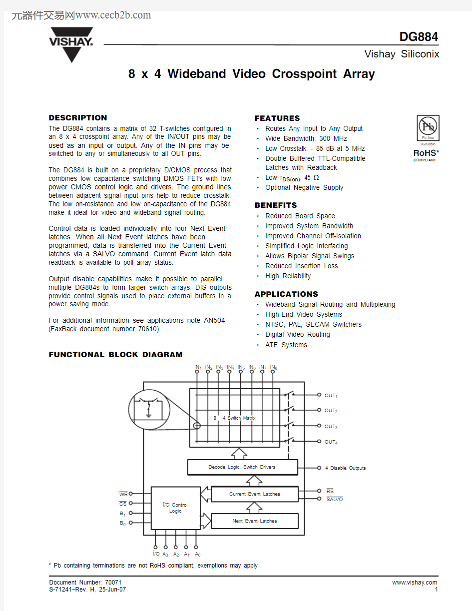
The DG884 contains a matrix of 32 T-switches configured in an 8 x 4 crosspoint array. Any of the IN/OUT pins may be used as an input or output. Any of the IN pins may be switched to any or simultaneously to all OUT pins.
The DG884 is built on a proprietary D/CMOS process that combines low capacitance switching DMOS FETs with low power CMOS control logic and drivers. The ground lines between adjacent signal input pins help to reduce crosstalk.The low on-resistance and low on-capacitance of the DG884make it ideal for video and wideband signal routing.Control data is loaded individually into four Next Event latches. When all Next Event latches have been programmed, data is transferred into the Current Event latches via a SALVO command. Current Event latch data readback is available to poll array status.
Output disable capabilities make it possible to parallel multiple DG884s to form larger switch arrays. DIS outputs provide control signals used to place external buffers in a power saving mode.
For additional information see applications note AN504(FaxBack document number 70610).
FUNCTIONAL BLOCK DIAGRAM
* Pb containing terminations are not RoHS compliant, exemptions may apply
Vishay Siliconix
DG884
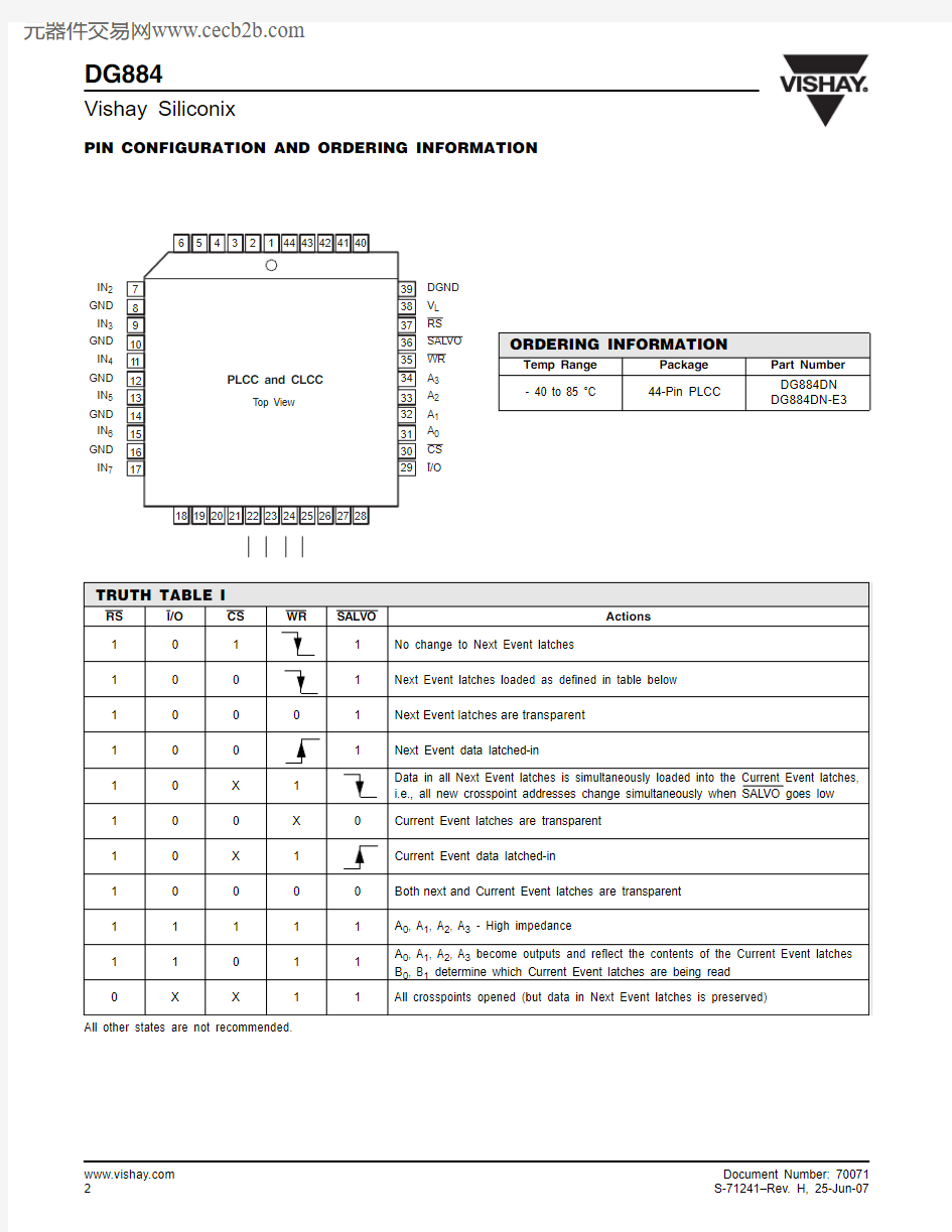
PIN CONFIGURATION AND ORDERING INFORMATION
All other states are not recommended.
ORDERING INFORMATION Temp Range Package
Part Number - 40 to 85 °C 44-Pin PLCC
DG884DN
DG884DN-E3
TRUTH TABLE I
RS I/O CS WR
SALVO Actions
1011No change to Next Event latches
1001Next Event latches loaded as defined in table below 10001Next Event latches are
transparent 1001
Next Event data latched-in
10X 1Data in all Next Event latches is simultaneously loaded into the Current Event latches, i.e., all new crosspoint addresses change simultaneously when SALVO goes low 100X 0
Current Event latches are transparent 10X 1Current Event data latched-in
10000Both next and Current Event latches are transparent 11111A 0, A 1, A 2, A 3 - High impedance
11011A 0, A 1, A 2, A 3 become outputs and reflect the contents of the Current Event latches B 0, B 1 determine which Current Event latches are being read 0
X
X
1
1All crosspoints opened (but data in Next Event latches is preserved)
Vishay Siliconix
DG884
Notes:
When WR = 0 Next Event latches are transparent. Each crosspoint is addressed individually, e.g., to connect IN 1 to OUT 1 thru OUT 4 requires A 0, A 1, A 2 = 0 to be latched with each combination of B 0, B 1Notes:
a. All leads soldered or welded to PC Board.
b. Derate 6 mW/°C above 75 °C
c. Derate 16 mW/°C above 75 °C. TRUTH TABLE II
WR
B 1
B 0
A 3
A 2A 1A 0Next Event Latches 0
000IN 1 to OUT 1 Loaded 001IN 2 to OUT 1 Loaded 010IN 3 to OUT 1 Loaded 011IN 4 to OUT 1 Loaded 001
100IN 5 to OUT 1 Loaded 101IN 6 to OUT 1 Loaded 110IN 7 to OUT 1 Loaded 111IN 8 to OUT 1 Loaded 0
X X X Turn Off
OUT 1 Loaded 000IN 1 to OUT 2 Loaded 001IN 2 to OUT 2 Loaded 010IN 3 to OUT 2 Loaded 011IN 4 to OUT 2 Loaded 011
100IN 5 to OUT 2 Loaded 101IN 6 to OUT 2 Loaded 110IN 7 to OUT 2 Loaded 111IN 8 to OUT 2 Loaded 0
X X X Turn Off
OUT 2 Loaded 000IN 1 to OUT 3 Loaded 001IN 2 to OUT 3 Loaded 010IN 3 to OUT 3 Loaded 011IN 4 to OUT 3 Loaded 101
100IN 5 to OUT 3 Loaded 101IN 6 to OUT 3 Loaded 110IN 7 to OUT 3 Loaded 111IN 8 to OUT 3 Loaded 0
X X X Turn Off
OUT 3 Loaded 000IN 1 to OUT 4 Loaded 001IN 2 to OUT 4 Loaded 010IN 3 to OUT 4 Loaded 011IN 4 to OUT 4 Loaded 111
100IN 5 to OUT 4 Loaded 101IN 6 to OUT 4 Loaded 110IN 7 to OUT 4 Loaded 111IN 8 to OUT 4 Loaded 0
X
X
X
Turn Off
OUT 4 Loaded
ABSOLUTE MAXIMUM RATINGS
Parameter Limit Unit
V+ to GND - 0.3 to 21V
V+ to V- - 0.3 to 21V- to GND - 10 to 0.3V L to GND 0 to (V+) + 0.3Digital Inputs (V-) - 0.3 to (V L ) + 0.3
or 20 mA, whichever occurs first
V S , V D
(V-) - 0.3 to (V-) + 14
or 20 mA, whichever occurs first
Current (any terminal) Continuous
20mA
Current (S or D) Pulsed 1 ms 10 % Duty
40Storage Temperature
(A Suffix)
- 65 to 150°C
(D Suffix)- 65 to 125Operating T emperature
(A Suffix)
- 55 to 125(D Suffix)
- 40 to 85Power Dissipation (Package)a
44-Pin Quad J Lead PLCC b
450mW
44-Pin Quad J Lead Hermetic CLCC c
1200
Vishay Siliconix
DG884
SPECIFICATIONS a
Parameter Symbol Test Conditions Unless Specified V+ = 15 V , V- = - 3 V V L = 5 V , RS = 2.0 V
SALVO, CS, WR, I/O = 0.8 V Temp b T
yp c A Suffix - 55 to 125 °C
D Suffix - 40 to 85 °C
Unit
Min d Max d Min d Max d Unit Analog Switch
Analog Signal Range e V ANALOG V- = - 5 V Full - 5
8- 5
8V Drain-Source
On-Resistance r DS(on)I S = - 10 mA, V D = 0 V V AIH = 2.0 V , V AIL = 0.8 V Sequence Each Switch On Room Full 459012090120Ω
Resistance Match Between Channels
Δr DS(on)Room 3
9
9
Source Off Leakage Current I S(off)V S = 8 V , V D = 0 V, RS = 0.8 V Room Full - 20- 20020200- 20- 20020200nA
Drain Off Leakage Current I D(off)V D = 0 V , V S = 8 V, RS = 0.8 V
Room Full - 20- 20020200- 20- 20020200Total Switch On Leakage Current I D(on)V S = V D = 8 V
Room Full - 20- 2000202000- 20- 20020200
Digital Input/Output Input Voltage High V AIH Full 22
V
Input Voltage Low V AIL Full 0.80.8Address Input Current I AI V AI = 0 V or 2 V or 5 V Room Full 0.1- 1- 10110- 1 - 10110μA
Address Output Current I AO V AO = 2.7 V , See T ruth Table Room - 600- 200
- 200
V AO = 0.4 V , See T ruth Table Room 1500500
500
DIS Pin Sink Current I DIS
Room
1.5mA
Dynamic Characteristics On State Input Capacitance e C S(on) 1 In to 1 Out, See Figure 11Room 3040pF
1 In to 4 Out, See Figure 11
Room 120160Off State Input Capacitance e C S(off)See Figure 11
Room 82020Off State Output Capacitance e C D(off)Room 10
20
20Transition Time
t TRANS See Figure 5
Room 300ns Break-Before-Make Interval t OPEN Full 1010SALVO, WR T urn On Time t ON R L = 1 k Ω, C L = 35 pF 50 % Control to 90 % Output
See Figure 3Room Full 300500300SALVO, WR T urn Off Time t OFF Room Full 175300
175
Charge Injection
Q See Figure 6Room - 100pC Matrix Disabled Crosstalk X TALK(DIS)R IN = R L = 75 Ω f = 5 MHz, See Figure 10Room - 82dB
Adjacent Input Crosstalk X T ALK(AI)R IN = 10 Ω, R L = 10 k Ω f = 5 MHz, See Figure 9Room - 85All Hostile Crosstalk X T ALK(AH)
R IN = 10 Ω, R L = 10 k Ω f = 5 MHz, See Figure 8Room - 66Bandwidth
BW
R L = 50 Ω, See Figure 7
Room
300
MHz
Vishay Siliconix
DG884
Notes:
a. Refer to PROCESS OPTION FLOWCHART.
b. Room = 25 °C, Full = as determined by the operating temperature suffix.
c. Typical values are for DESIGN AID ONLY, not guaranteed nor subject to production testing.
d. The algebraic convention whereby the most negative value is a minimum and the most positive a maximum, is used in this data sheet.
e. Guaranteed by design, not subject to production test.
Stresses beyond those listed under “Absolute Maximum Ratings” may cause permanent damage to the device. These are stress ratings only, and functional operation of the device at these or any other conditions beyond those indicated in the operational sections of the specifications is not implied. Exposure to absolute maximum rating conditions for extended periods may affect device reliability.
SPECIFICATIONS a
Parameter Symbol Test Conditions Unless Specified V+ = 15 V , V- = - 3 V V L = 5 V , RS = 2.0 V
SALVO, CS, WR, I/O = 0.8 V Temp b T yp c A Suffix - 55 to 125 °C
D Suffix - 40 to 85 °C
Unit
Min d Max d Min d Max d
Unit
Power Supplies Positive Supply Current I+All Inputs at GND or 2 V
RS = 2 V
Room Full 1.536
36
mA
Negative Supply Current I-Room Full - 1.5- 3- 5- 3- 5Digital GND Supply Current I DG Full - 275- 750
- 750
μA
Logic Supply Current I L Full 200
500500Functional Operating Supply Voltage Range e
V+ to V-See Operating Voltage Range (T ypical Characteristics) page 6
Full 13201320V
V- to GND Full - 5.50- 5.50V+ to GND
Full 1020
1020
Minimum Input Timing Requirements Address Write Time t AW See Figure 1
Full 205050ns
Minimum WR Pulse Width
t WP Full 50100100Write Address Time t WA Full - 101010Chip Select Write Time t CW Full 50100100Write Chip Select Time t WC Full 257575Minimum SALVO Pulse Width t SP Full 50100100SALVO Write Time t SW Full - 10
1010Write SALVOTime t WS Room 2050Input Output Time t IO Room 150200200Address Output Time t AO Room 150200200Chip Select Output Time t CO Room 150200
200Chip Select Address Time t CA Room 60
100Reset to SALVO t RS Full 5050
I/O Address Input Time
t IA
Room
50
Vishay Siliconix
DG884
TYPICAL CHARACTERISTICS 25 °C, unless otherwise noted
Matrix Disabled Crosstalk Operating Voltage Area
Vishay Siliconix
DG884
TIMING DIAGRAMS
Figure 2. Output Timing Requirements
PARAMETER DEFINITIONS
Symbol Parameter Description
T AW Address to Write Minimum time address must be valid before WR goes high T WA Write to Address Minimum time address must remain valid after WR pulse goes high T WP WR Pulse Minimum time of WR pulse width to write address into Next Event latches T CW Chip Select to WR Minimum time chip select must be valid before a WR pulse T WC WR to Chip Select Minimum time chip select must remain valid after WR pulse T SP SALVO Pulse Minimum time of SALVO pulse width
T WS WR to SALVO Minimum time from WR pulse to SALVOto load new address T SW SALVO to WR Minimum time from SALVO pulse to WR to load current address T IA I/O to Address In Minimum time I/O must be valid before address applied T RS RS to SALVO Minimum time RS must be valid before SALVO pulse T IO I/O to Output Minimum time I/O must be valid before address output valid T AO Address to Output Minimum time address B X must be valid until address A X output valid T CO CS to Output Minimum time CS must be valid until A X output is valid
T CA
CS to Address In
Minimum time CS must be valid before address applied if I/O is high
DG884
Vishay Siliconix
TEST CIRCUITS
Figure 3. SALVO Turn On/Off Time
Figure 4. WR Turn On/Off Time
Figure 5. Transition Time and Break-Before-Make Interval
Vishay Siliconix
DG884
TEST CIRCUITS
Figure 6. Charge Injection Figure 8. All Hostile Crosstalk Figure 10. Matrix Disabled Crosstalk
Figure 7. -3 dB Bandwidth
Figure 9. Adjacent Input Crosstalk
Figure 11. On-State and Off-State Capacitances
Vishay Siliconix DG884
DEVICE DESCRIPTION
The DG884 is the world’s first monolithic wideband crosspoint array that operates from dc to > 100 MHz. The DG884 offers the ability to route any one of eight input signals to any one of four OUT pins. Any input can be routed to one, two, three or four OUTs simultaneously with no risk of shorting inputs together (guaranteed by design).
Each crosspoint is configured as a “T” switch in which DMOS FETs are used due to their excellent low resistance and low capacitance characteristics. Each OUT line has a series switch that minimizes capacitive loading when the OUT is off. Interfacing
The DG884 was designed to allow complex matrices to be developed while maintaining a simple control interface. The status of the I/O pin determines whether the DG884 is being written to or read from (see Figures 1 and 2).
be low, while RS, WR and SALVO must be high. The IN to OUT path is selected by using address A0 through A3 to define the IN line and address B0 and B1 to define the OUT line. That is, The IN defined by A0 through A3 is electrically connected to the OUT defined by B0, B1. This chosen path is returns high again. This operation is repeated up to three more times if other crosspoint connections need to be changed.Upon completing all crosspoint connections that are to be changed in a single device, other DG884s can be similarly preset by taking the CS pin low on the appropriate device. When all DG884s are preset, the Current Event latches are simultaneously changed by a single SALVO command applied to all devices. In this manner the crosspoint configuration of any number of devices can be simultaneously updated.
Four open drain disable OUTs are provided to control external line drivers or to provide visual or electrical signaling. For example, any or all of the DIS OUTs can directly interface with a CLC410 Video Amplifier to place it into a high impedance, low-power standby mode when the corresponding OUT is not being used. (See Figure 15). The
is open or RS is low.
Reset
The reset function (RS) allows the resetting of all crosspoints to a known state (open). At power up, the reset facility may be used to guarantee that all switches are open. It should be Event latches remain unchanged. This useful facility allows the user to return the matrix to its previous state (prior to reset) by simply applying the SALVO command. Alternatively, the user can reprogram the Next Event latches, and then apply the SALVO command to reconfigure the matrix to a new state.
PIN DESCRIPTION
Pin Symbol Description 1, 3, 4, 6, 8, 10, 12, 14,
16, 18, 20, 41, 43
GND Analog Signal Ground
39DGND Digital Ground
26V+Positive Supply Voltage
21V-Negative Supply Voltage
38V L Logic Supply Voltage - generally 5 V
5, 7, 9, 11, 13, 15, 17, 19IN1 to IN88 Analog Input Channels
2, 40, 42, 44OUT1 to OUT4 4 Analog Output Channels
29I/O Determines whether data is being written into the Next Event latches or read from the Current Event latches
30CS Chip Select - a logic input
31, 32, 33, 34A0, A1, A2, A3IN Address - logic inputs or outputs as defined by I/O pin, select one of eight IN channels 27, 28B0, B1OUT Address - logic inputs, select one of four OUT channels
35WR Write command that latches A0, A1, A2, A3 into the Next Event latches
36SALVO Master write command, that in one action, transfers all the data from Next Event latches into Current Event latches
37RS Reset - a low will clear the Current Event latches
22, 23, 24, 25DIS1 to DIS4Open drain disable outputs - these outputs pull low when the corresponding OUT channel is off
Vishay Siliconix
DG884
DEVICE DESCRIPTION
Readback
The I/O facility enables the user to write data to the Next Event latches or to read the contents of the Current Event latches. This feature permits the central controller to periodically monitor the state of the matrix. If a power loss to
the controller occurs, the readback feature helps the matrix to recover rapidly. It also offers a means to perform PC board diagnostics both in production and in system operation.
APPLICATIONS
Figure 12. Control Circuitry
Figure 13. Fully Buffered 8 x 4 Crosspoint
Vishay Siliconix
DG884
APPLICATIONS
Power Supplies and Decoupling
A useful feature of the DG884 is its power supply flexibility. It
can be operated from dual supplies, or a single positive supply (V- connected to 0 V) if required. Allowable operating voltage ranges are shown in Operating Voltage Range (Typical Characteristics) graph, page 6.
Note that the analog signal must not go below V- by more than 0.3 V (see absolute maximum ratings). However, the addition of a V- pin has a number of advantages:1)
It allows flexibility in analog signal handling, i.e. with V- = - 5 V and V+ = 15 V, up to ± 5 V ac signals can be accepted.
2)
The value of on-capacitance [C S(on)] may be reduced by increasing the value of V-. It is useful to note that optimum video differential phase and gain occur when V- is - 3 V. Note that V+ has no effect on C S(on).3)
V- eliminates the need to bias an ac analog signal using potential dividers and large decoupling capacitors.
It is established RF design practice to incorporate sufficient bypass capacitors in the circuit to decouple the power supplies to all active devices in the circuit. The dynamic performance of the DG 884 is adversely affected by poor decoupling of power supply pins. Also, since the substrate of the device is connected to the negative supply, proper decoupling of this pin is essential.
Rules:1) Decoupling capacitors should be incorporated on all power supply pins (V+, V-, V L ).
2) They should be mounted as close as possible to the device pins.
3)
Capacitors should have good high frequency characteristics - tantalum bead and/or monolithic ceramic disc types are suitable.
Recommended decoupling capacitors are 1 to 10 μF tantalum bead, in parallel with 100 nF monolithic ceramic.4)
Additional high frequency protection may be provided by 51 Ω carbon film resistors connected in series with the power supply pins (see Figure 14).
The V L pin permits interface to various logic types. The device is primarily designed to be TTL or CMOS logic compatible with + 5 V applied to V L . The actual logic threshold can be raised simply by increasing V L .
Figure 14. DG884 Power Supply Decoupling
Figure 15. Switching Threshold Voltage vs. V L
Vishay Siliconix
DG884
APPLICATIONS
A typical switching threshold versus V L is shown in Figure 15.These devices feature an address readback facility whereby the last address written to the device may be read by the system. This allows improved status monitoring and hand shaking without additional external components.
When the I/O assigns the address output condition, the A X address pins can sink or source current for logic low and high, respectively. Note that V L is the logic high output condition. This point must be respected if V L is varied for input logic threshold shifting.
Note: Even though these devices are designed to be latchup resistant, V L must not exceed V+ by more than 0.3 V in operation or during power supply on/off sequencing.
Layout
The PLCC package pinout is optimized so that large crosspoint arrays can be easily implemented with a minimum number of PCB layers (see Figure 16). Crosstalk is minimized and off-isolation is optimized by having ground pins located adjacent to each input and output signal pins.Optimum off-isolation and low crosstalk performance can only be achieved by the proper use of RF layout techniques:avoid sockets, use ground planes, avoid ground loops,bypass the power supplies with high frequency type capacitors (low ESR, low ESL), use striplines to maintain transmission line impedance matching.
Vishay Silico nix maintains wo rldwide manufacturing capability. Pro ducts may be manufactured at o ne o f several qualified lo catio ns. Reliability data fo r Silico n Technology and Package Reliability represent a composite of all qualified locations. For related documents such as package/tape drawings, part marking, and reliability data, see https://www.360docs.net/doc/1015232455.html,/ppg?70071.
Figure 16. 16 X 8 Expandable Crosspoint Matrix Using DG884
Disclaimer Legal Disclaimer Notice
Vishay
All product specifications and data are subject to change without notice.
Vishay Intertechnology, Inc., its affiliates, agents, and employees, and all persons acting on its or their behalf (collectively, “Vishay”), disclaim any and all liability for any errors, inaccuracies or incompleteness contained herein or in any other disclosure relating to any product.
Vishay disclaims any and all liability arising out of the use or application of any product described herein or of any information provided herein to the maximum extent permitted by law. The product specifications do not expand or otherwise modify Vishay’s terms and conditions of purchase, including but not limited to the warranty expressed therein, which apply to these products.
No license, express or implied, by estoppel or otherwise, to any intellectual property rights is granted by this document or by any conduct of Vishay.
The products shown herein are not designed for use in medical, life-saving, or life-sustaining applications unless otherwise expressly indicated. Customers using or selling Vishay products not expressly indicated for use in such applications do so entirely at their own risk and agree to fully indemnify Vishay for any damages arising or resulting from such use or sale. Please contact authorized Vishay personnel to obtain written terms and conditions regarding products designed for such applications.
Product names and markings noted herein may be trademarks of their respective owners.
元器件交易网https://www.360docs.net/doc/1015232455.html,