TMS320x2833x Multichannel Buffered Serial Port (McBSP) Reference Guide 第七章 外文
第7章Receiver Configuration
To configure the McBSP receiver, perform the following procedure:
1. Place the McBSP/receiver in reset (see Section 7.2).
2. Program McBSP registers for the desired receiver operation (see Section 7.1).
3. Take the receiver out of reset (see Section 7.2).
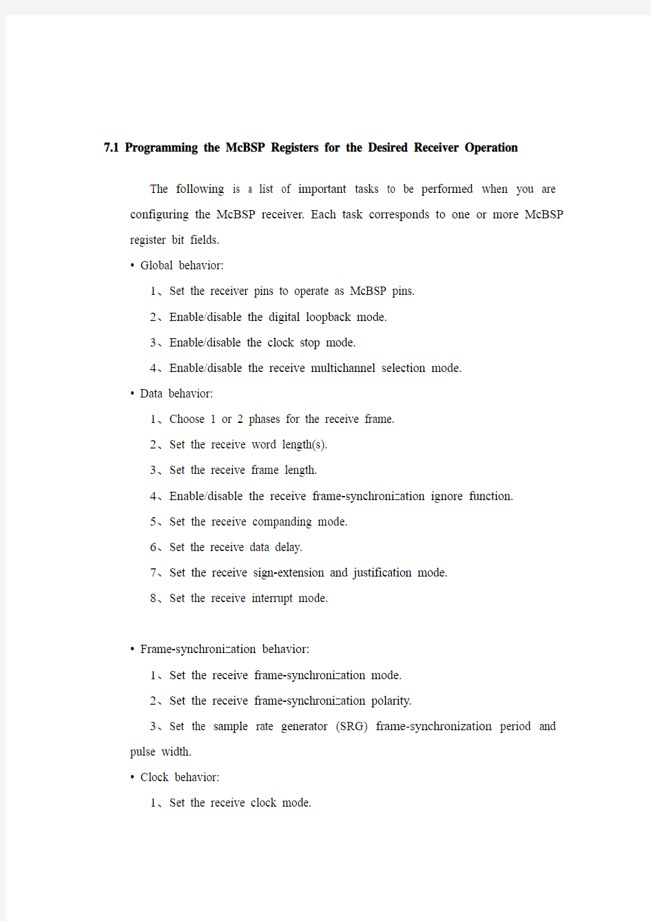
7.1 Programming the McBSP Registers for the Desired Receiver Operation
The following is a list of important tasks to be performed when you are configuring the McBSP receiver. Each task corresponds to one or more McBSP register bit fields.
? Global behavior:
1、Set the receiver pins to operate as McBSP pins.
2、Enable/disable the digital loopback mode.
3、Enable/disable the clock stop mode.
4、Enable/disable the receive multichannel selection mode.
? Data behavior:
1、Choose 1 or 2 phases for the receive frame.
2、Set the receive word length(s).
3、Set the receive frame length.
4、Enable/disable the receive frame-synchronization ignore function.
5、Set the receive companding mode.
6、Set the receive data delay.
7、Set the receive sign-extension and justification mode.
8、Set the receive interrupt mode.
? Frame-synchronization behavior:
1、Set the receive frame-synchronization mode.
2、Set the receive frame-synchronization polarity.
3、Set the sample rate generator (SRG) frame-synchronization period and
pulse width.
? Clock behavior:
1、Set the receive clock mode.
2、Set the receive clock polarity.
3、Set the SRG clock divide-down value.
4、Set the SRG clock synchronization mode.
5、Set the SRG clock mode (choose an input clock).
7.2 Resetting and Enabling the Receiver
The first step of the receiver configuration procedure is to reset the receiver, and the last step is to enable the receiver (to take it out of reset). Table 7-1 describes the bits used for both of these steps.
7.2.1 Reset Considerations
The serial port can be reset in the following two ways:
1. The DSP reset (XRS signal driven low) places the receiver, transmitter, and sample rate generator in reset. When the device reset is removed (XRS signal released), GRST = FRST = RRST = XRST = 0 keep the entire serial port in the reset state.
2. The serial port transmitter and receiver can be reset directly using the RRST and XRST bits in the serial port control registers. The sample rate generator can be reset directly using the GRST bit in SPCR2.
Table 7-2 shows the state of McBSP pins when the serial port is reset due to a device reset and a direct receiver/transmitter reset.
For more details about McBSP reset conditions and effects, see Section 9.2, Resetting and Initializing a McBSP.
7.3 Set the Receiver Pins to Operate as McBSP Pins
To configure a pin for its McBSP function , you should configure the bits of the GPxMUXn register appropriately. In addition to this, bits 12 and 13 of the PCR register must be set to 0. These bits are defined as reserved.
7.4 Enable/Disable the Digital Loopback Mode
The DLB bit determines whether the digital loopback mode is on. DLB is described in Table 7-3.
7.4.1 Digital Loopback Mode
In the digital loopback mode, the receive signals are connected internally through
multiplexers to the corresponding transmit signals, as shown in Table 7-4. This mode allows testing of serial port code with a single DSP device; the McBSP receives the data it transmits.
Table 7-4. Receive Signals Connected to Transmit Signals in Digital Loopback Mode
7.5 Enable/Disable the Clock Stop Mode
The CLKSTP bits determine whether the clock stop mode is on. CLKSTP is described in Table 7-5.
Table 7-5. Register Bits Used to Enable/Disable the Clock Stop Mode
7.5.1 Clock Stop Mode
The clock stop mode supports the SPI master-slave protocol. If you do not plan to use the SPI protocol, you can clear CLKSTP to disable the clock stop mode.
In the clock stop mode, the clock stops at the end of each data transfer. At the beginning of each data transfer, the clock starts immediately (CLKSTP = 10b) or after a half-cycle delay (CLKSTP = 11b). The CLKXP bit determines whether the starting edge of the clock on the MCLKX pin is rising or falling. The CLKRP bit determines whether receive data is sampled on the rising or falling edge of the clock shown on the MCLKR pin.
Table 7-6 summarizes the impact of CLKSTP, CLKXP, and CLKRP on serial port
operation. In the clock stop mode, the receive clock is tied internally to the transmit clock, and the receive frame-synchronization signal is tied internally to the transmit frame-synchronization signal.
Table 7-6. Effects of CLKSTP, CLKXP, and CLKRP on the Clock Scheme
7.6 Enable/Disable the Receive Multichannel Selection Mode
The RMCM bit determines whether the receive multichannel selection mode is on. RMCM is described in Table 7-7. For more details, see Section 5.6, Receive Multichannel Selection Mode.
Table 7-7. Register Bit Used to Enable/Disable the Receive Multichannel
7.7 Choose One or Two Phases for the Receive Frame
The RPHASE bit (see Table 7-8) determines whether the receive data frame has one or two phases.
Table 7-8. Register Bit Used to Choose One or Two Phases for the Receive
Frame
7.8 Set the Receive Word Length(s)
The RWDLEN1 and RWDLEN2 bit fields (see Table 7-9) determine how many bits are in each serial word in phase 1 and in phase 2, respectively, of the receive data frame.
Table 7-9. Register Bits Used to Set the Receive Word Length(s)
7.8.1 Word Length Bits
Each frame can have one or two phases, depending on the value that you load into the RPHASE bit. If a single-phase frame is selected, RWDLEN1 selects the length for every serial word received in the frame. If a dual-phase frame is selected, RWDLEN1 determines the length of the serial words in phase 1 of the frame and RWDLEN2 determines the word length in phase 2 of the frame.
7.9 Set the Receive Frame Length
The RFRLEN1 and RFRLEN2 bit fields (see Table 7-10) determine how many serial words are in phase 1 and in phase 2, respectively, of the receive data frame.
7.9.1 Selected Frame Length
The receive frame length is the number of serial words in the receive frame. Each frame can have one or two phases, depending on value that you load into the RPHASE bit.
If a single-phase frame is selected (RPHASE = 0), the frame length is equal to the
length of phase 1. If a dual-phase frame is selected (RPHASE = 1), the frame length is the length of phase 1 plus the length of phase 2.
The 7-bit RFRLEN fields allow up to 128 words per phase. See Table 7-11 for a summary of how to calculate the frame length. This length corresponds to the number of words or logical time slots or channels per frame-synchronization pulse.
Program the RFRLEN fields with [w minus 1], where w represents the number of words per phase. For the example, if you want a phase length of 128 words in phase 1, load 127 into RFRLEN1.
7.10 Enable/Disable the Receive Frame-Synchronization Ignore Function
The RFIG bit (see Table 7-12) controls the receive frame-synchronization ignore function.
7.10.1 Unexpected Frame-Synchronization Pulses and the Frame-Synchronization Ignore Function
If a frame-synchronization pulse starts the transfer of a new frame before the current frame is fully received, this pulse is treated as an unexpected frame-synchronization pulse. When RFIG = 1, reception continues, ignoring the unexpected frame-synchronization pulses.
When RFIG = 0, an unexpected FSR pulse causes the McBSP to discard the contents of RSR[1,2] in favor of the new incoming data. Therefore, if RFIG = 0 and an unexpected frame-synchronization pulse occurs, the serial port:
1. Aborts the current data transfer
2. Sets RSYNCERR in SPCR1 to 1
3. Begins the transfer of a new data word
For more details about the frame-synchronization error condition, see Section 4.3, Unexpected Receive Frame-Synchronization Pulse.
7.10.2 Examples of Effects of RFIG
Figure 7-1 shows an example in which word B is interrupted by an unexpected frame-synchronization pulse when (R/X)FIG = 0. In the case of reception, the reception of B is aborted (B is lost), and a new data word in this example) is received after the appropriate data delay. This condition is a receive synchronization error, which sets the RSYNCERR bit.
Figure 7-1. Unexpected Frame-Synchronization Pulse With (R/X)FIG = 0
In contrast with Figure 7-1, Figure 7-2 shows McBSP operation when unexpected frame-synchronization signals are ignored (when (R/X)FIG = 1). Here, the transfer of word B is not affected by an unexpected pulse.
Figure 7-2. Unexpected Frame-Synchronization Pulse With (R/X)FIG = 1
7.11 Set the Receive Companding Mode
The RCOMPAND bits (see Table 7-13) determine whether companding or another data transfer option is chosen for McBSP reception.
Table 7-13. Register Bits Used to Set the Receive Companding Mode
(continued)
7.11.1 Companding
Companding (COMpressing and exPANDing) hardware allows compression and expansion of data in either μ-law or A-law format. The companding standard employed in the United States and Japan is μ-law. The European companding standard is referred to as A-law. The specifications for μ-law and A-law log PCM are part of the CCITT G.711 recommendation.
A-law and μ-law allow 13 bits and 14 bits of dynamic range, respectively. Any values outside this range are set to the most positive or most negative value. Thus, for companding to work best, the data transferred to and from the McBSP via the CPU or DMA controller must be at least 16 bits wide.
The μ-law and A-law formats both encode data into 8-bit code words. Companded data is always 8 bits wide; the appropriate word length bits (RWDLEN1, RWDLEN2, XWDLEN1, XWDLEN2) must therefore be set to 0, indicating an 8-bit wide serial data stream. If companding is enabled and either of the frame phases does
not have an 8-bit word length, companding continues as if the word length is 8 bits.
Figure 7-3 illustrates the companding processes. When companding is chosen for the transmitter, compression occurs during the process of copying data from DXR1 to XSR1. The transmit data is encoded according to the specified companding law (A-law or μ-law). When companding is chosen for the receiver, expansion occurs during the process of copying data from RBR1 to DRR1. The receive data is decoded to 2's-complement format.
Figure 7-3. Companding Processes for Reception and for Transmission
7.11.2 Format of Expanded Data
For reception, the 8-bit compressed data in RBR1 is expanded to left-justified 16-bit data in DRR1. The RJUST bit of SPCR1 is ignored when companding is used.
7.11.3 Companding Internal Data
If the McBSP is otherwise unused (the serial port transmit and receive sections are reset), the companding hardware can compand internal data. See Section 2.2.2, Capability to Compand Internal Data.
7.11.4 Option to Receive LSB First
Normally, the McBSP transmits or receives all data with the most significant bit (MSB) first. However, certain 8-bit data protocols (that do not use companded data) require the least significant bit (LSB) to be transferred first. If you set RCOMPAND = 01b in RCR2, the bit ordering of 8-bit words is reversed during reception. Similar to companding, this feature is enabled only if the appropriate word length bits are set to 0, indicating that 8-bit words are to be transferred serially. If either phase of the frame
does not have an 8-bit word length, the McBSP assumes the word length is eight bits and LSB-first ordering is done.
7.12 Set the Receive Data Delay
7.12.1 Data Delay
The start of a frame is defined by the first clock cycle in which frame synchronization is found to be active. The beginning of actual data reception or transmission with respect to the start of the frame can be delayed if required. This delay is called data delay.
RDATDLY specifies the data delay for reception. The range of programmable data delay is zero to two bit-clocks (RDATDLY = 00b-10b), as described in Table 7-14 and shown in Figure 7-4. In this figure, the data transferred is an 8-bit value with bits labeled B7, B6, B5, and so on. Typically a 1-bit delay is selected, because data often follows a 1-cycle active frame-synchronization pulse.
7.12.2 0-Bit Data Delay
Normally, a frame-synchronization pulse is detected or sampled with respect to an edge of internal serial clock CLK(R/X). Thus, on the following cycle or later (depending on the data delay value), data may be received or transmitted. However, in the case of 0-bit data delay, the data must be ready for reception and/or transmission on the same serial clock cycle.
For reception, this problem is solved because receive data is sampled on the first
falling edge of MCLKR where an active-high internal FSR is detected. However, data transmission must begin on the rising edge of the internal CLKX clock that generated the frame synchronization. Therefore, the first data bit is assumed to be present in XSR1, and thus on DX. The transmitter then asynchronously detects the frame-synchronization signal (FSX) going active high and immediately starts driving the first bit to be transmitted on the DX pin.
Figure 7-4. Range of Programmable Data Delay
7.12.3 2-Bit Data Delay
A data delay of two bit periods allows the serial port to interface to different types of T1 framing devices where the data stream is preceded by a framing bit. During reception of such a stream with data delay of two bits (framing bit appears after a 1-bit delay and data appears after a 2-bit delay), the serial port essentially discards the framing bit from the data stream, as shown in Figure 7-5. In this figure, the data transferred is an 8-bit value with bits labeled B7, B6, B5, and so on.
Figure 7-5. 2-Bit Data Delay Used to Skip a Framing Bit
7.13 Set the Receive Sign-Extension and Justification Mode
The RJUST bits (see Table 7-15) determine whether data received by the McBSP is sign-extended and how it is justified.
7.13.1 Sign-Extension and the Justification
RJUST in SPCR1 selects whether data in RBR[1,2] is right-or left-justified (with respect to the MSB) in DRR[1,2] and whether unused bits in DRR[1,2] are filled with zeros or with sign bits.
Table 7-16 and Table 7-17 show the effects of various RJUST values. The first table shows the effect on an example 12-bit receive-data value ABCh. The second table shows the effect on an example 20-bit receive-data value ABCDEh.
Table 7-17. Example: Use of RJUST Field With 20-Bit Data Value ABCDEh
7.14 Set the Receive Interrupt Mode
The RINTM bits (see Table 7-18) determine which event generates a receive interrupt request to the CPU.
The receive interrupt (RINT) informs the CPU of changes to the serial port status. Four options exist for configuring this interrupt. The options are set by the receive interrupt mode bits, RINTM, in SPCR1.
7.15 Set the Receive Frame-Synchronization Mode
The bits described in Table 7-19 determine the source for receive frame synchronization and the function of the FSR pin.
7.15.1 Receive Frame-Synchronization Modes
Table 7-20 shows how you can select various sources to provide the receive
frame-synchronization signal and the effect on the FSR pin. The polarity of the signal on the FSR pin is determined by the FSRP bit.
In digital loopback mode (DLB = 1), the transmit frame-synchronization signal is used as the receive frame-synchronization signal.
Also in the clock stop mode, the internal receive clock signal (MCLKR) and the internal receive frame-synchronization signal (FSR) are internally connected to their transmit counterparts, CLKX and FSX.
Table 7-19. Register Bits Used to Set the Receive Frame Synchronization Mode
Table 7-20. Select Sources to Provide the Receive Frame-Synchronization Signal
and the Effect onthe FSR Pin (continued)
7.16 Set the Receive Frame-Synchronization Polarity
The FSRP bit (see Table 7-21) determines whether frame-synchronization pulses are active high or active low on the FSR pin.
Table 7-21. Register Bit Used to Set Receive Frame-Synchronization Polarity
7.16.1 Frame-Synchronization Pulses, Clock Signals, and Their Polarities
Receive frame-synchronization pulses can be generated internally by the sample rate generator (see Section 3.2) or driven by an external source. The source of frame synchronization is selected by programming the mode bit, FSRM, in PCR. FSR is also affected by the GSYNC bit in SRGR2. For information about the effects of FSRM and GSYNC, see Section 7.15, Set the Receive Frame-Synchronization Mode. Similarly, receive clocks can be selected to be inputs or outputs by programming the mode bit, CLKRM, in the PCR (see Section 7.17, Set the Receive Clock Mode).
When FSR and FSX are inputs (FSXM = FSRM= 0, external frame-synchronization pulses), the McBSP detects them on the internal falling edge of clock, internal MCLKR, and internal CLKX, respectively. The receive data arriving at the DR pin is also sampled on the falling edge of internal MCLKR. These internal clock signals are either derived from an external source via CLK(R/X) pins or driven by the sample rate generator clock (CLKG) internal to the McBSP.
When FSR and FSX are outputs, implying that they are driven by the sample rate generator, they are generated (transition to their active state) on the rising edge of the internal clock, CLK(R/X). Similarly, data on the DX pin is output on the rising edge of internal CLKX.
FSRP, FSXP, CLKRP, and CLKXP in the pin control register (PCR) configure the polarities of the FSR, FSX, MCLKR, and CLKX signals, respectively. All frame-synchronization signals (internal FSR, internal FSX) that are internal to the serial port are active high. If the serial port is configured for external frame synchronization (FSR/FSX are inputs to McBSP), and FSRP = FSXP = 1, the external active-low frame-synchronization signals are inverted before being sent to the receiver (internal FSR) and transmitter (internal FSX). Similarly, if internal synchronization (FSR/FSX are output pins and GSYNC = 0) is selected, the internal active-high frame-synchronization signals are inverted, if the polarity bit FS(R/X)P = 1, before being sent to the FS(R/X) pin.
On the transmit side, the transmit clock polarity bit, CLKXP, sets the edge used to
shift and clock out transmit data. Data is always transmitted on the rising edge of internal CLKX. If CLKXP = 1 and external clocking is selected (CLKXM = 0 and CLKX is an input), the external falling-edge triggered input clock on CLKX is inverted to a rising-edge triggered clock before being sent to the transmitter. If CLKXP = 1, and internal clocking selected (CLKXM = 1 and CLKX is an output pin), the internal (rising-edge triggered) clock, internal CLKX, is inverted before being sent out on the MCLKX pin.
Similarly, the receiver can reliably sample data that is clocked with a rising edge clock (by the transmitter). The receive clock polarity bit, CLKRP, sets the edge used to sample received data. The receive data is always sampled on the falling edge of internal MCLKR. Therefore, if CLKRP = 1 and external clocking is selected (CLKRM = 0 and MCLKR is an input pin), the external rising-edge triggered input clock on MCLKR is inverted to a falling-edge triggered clock before being sent to the receiver. If CLKRP = 1 and internal clocking is selected (CLKRM = 1), the internal falling-edge triggered clock is inverted to a rising-edge triggered clock before being sent out on the MCLKR pin.
MCLKRP = CLKXP in a system where the same clock (internal or external) is used to clock the receiver and transmitter. The receiver uses the opposite edge as the transmitter to ensure valid setup and hold of data around this edge. Figure 7-6 shows how data clocked by an external serial device using a rising edge can be sampled by the McBSP receiver on the falling edge of the same clock.
Figure 7-6. Data Clocked Externally Using a Rising Edge and Sampled by the
McBSP Receiver on aFalling Edge
Set the SRG Frame-Synchronization Period and Pulse Width