9308W中文资料
TL F 102089308 DM9308Dual 4-Bit Latch
June 1989
9308 DM9308Dual 4-Bit Latch
General Description
The 9308is a dual 4-bit D-type latch designed for general purpose storage applications in digital systems Each latch contains both an active LOW Master Reset input an active LOW Enable inputs The 74116is a pin for pin equivalent of the 9308
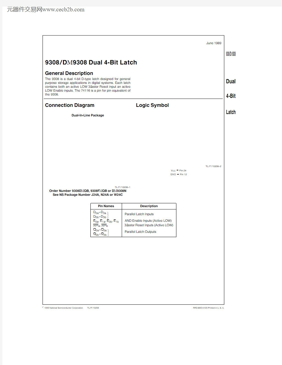
Connection Diagram
Dual-In-Line Package
TL F 10208–1
Order Number 9308DMQB 9308FMQB or DM9308N See NS Package Number J24A N24A or W24C
Logic Symbol
TL F 10208–2
V CC e Pin 24GND e Pin 12
Pin Names Description
D 0a –D 3a Parallel Latch Inputs
D 0b –D 3b
(
E 0a E 1a E 0b E 1b AND Enable Inputs (Active LOW)MR a MR b Master Reset Inputs (Active LOW)Q 0a –Q 3a Parallel Latch Outputs
Q 0b –Q 3b
(
C 1995National Semiconductor Corporation RRD-B30M105 Printed in U S A
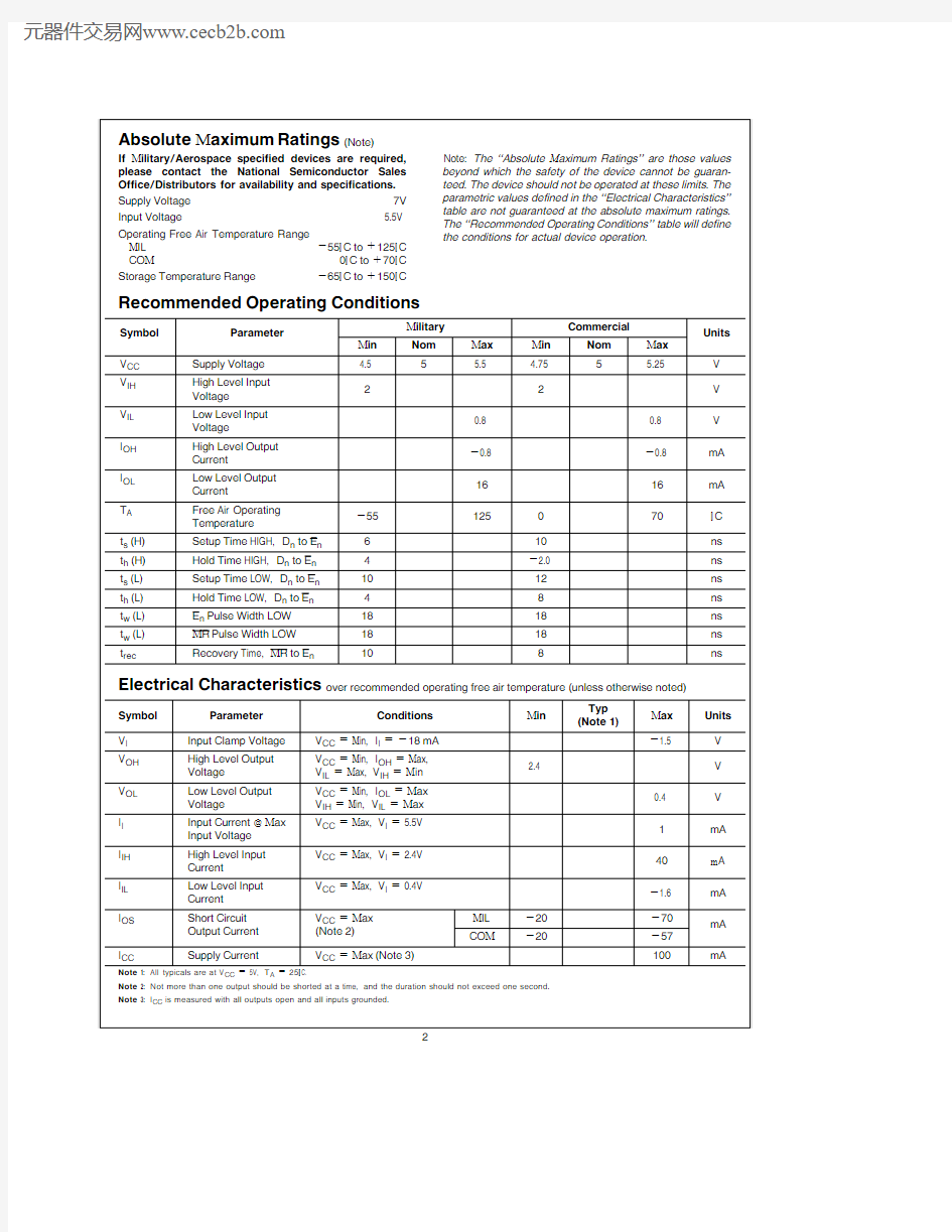
Absolute Maximum Ratings(Note)
If Military Aerospace specified devices are required please contact the National Semiconductor Sales Office Distributors for availability and specifications Supply Voltage7V Input Voltage5 5V Operating Free Air Temperature Range
MIL b55 C to a125 C COM0 C to a70 C Storage Temperature Range b65 C to a150 C Note The‘‘Absolute Maximum Ratings’’are those values beyond which the safety of the device cannot be guaran-teed The device should not be operated at these limits The parametric values defined in the‘‘Electrical Characteristics’’table are not guaranteed at the absolute maximum ratings The‘‘Recommended Operating Conditions’’table will define the conditions for actual device operation
Recommended Operating Conditions
Symbol Parameter
Military Commercial
Units Min Nom Max Min Nom Max
V CC Supply Voltage4 555 54 7555 25V
V IH High Level Input
22V Voltage
V IL Low Level Input
0 80 8V
Voltage
I OH High Level Output b
0 8b0 8mA
Current
I OL Low Level Output
1616mA Current
T A Free Air Operating b
55125070 C Temperature
t s(H)Setup Time HIGH D n to E n610ns
t h(H)Hold Time HIGH D n to E n4b2 0ns
t s(L)Setup Time LOW D n to E n1012ns
t h(L)Hold Time LOW D n to E n48ns
t w(L)E n Pulse Width LOW1818ns
t w(L)MR Pulse Width LOW1818ns
t rec Recovery Time MR to E n108ns Electrical Characteristics over recommended operating free air temperature(unless otherwise noted)
Symbol Parameter Conditions Min
Typ
Max Units (Note1)
V I Input Clamp Voltage V CC e Min I I e b18mA b1 5V
V OH High Level Output V CC e Min I OH e Max
2 4V
Voltage V IL e Max V IH e Min
V OL Low Level Output V CC e Min I OL e Max
0 4V
Voltage V IH e Min V IL e Max
I I Input Current Max V CC e Max V I e5 5V
1mA Input Voltage
I IH High Level Input V CC e Max V I e2 4V
40m A Current
I IL Low Level Input V CC e Max V I e0 4V b
1 6mA
Current
I OS Short Circuit V CC e Max MIL b20b70
mA Output Current(Note2)COM b20b57
I CC Supply Current V CC e Max(Note3)100mA Note1 All typicals are at V CC e5V T A e25 C
Note2 Not more than one output should be shorted at a time and the duration should not exceed one second
Note3 I CC is measured with all outputs open and all inputs grounded
2
Functional Description
Data can be entered into the latch when both of the enable inputs are LOW As long as this logic condition exists the output of the latch will follow the input If either of the enable inputs goes HIGH the data present in the latch at that time is held in the latch and is no longer affected by data input The master reset overrides all other input conditions and forces the outputs of all the latches LOW when a LOW sig-nal is applied to the Master Reset input Truth Table
MR E0E1D Qn Operation
H L L L L Data Entry
H L L H H Data Entry
H L H X Qn b1Hold
H H L X Qn b1Hold
H H H X Qn b1Hold
L X X X L Reset
Q n b1e Previous Output State
Q n e Present Output State
H e HIGH Voltage Level
L e LOW Voltage Level
X e Immaterial
Logic Diagram
TL F 10208–3
Switching Characteristics V CC e a5 0V T A e a25 C(See Section5for test waveforms and output load )
9308
Symbol Parameter
C L e15pF
Units R L e400X
Min Max
t PLH Propagation Delay30
ns t PHL En to Qn22
t PLH Propagation Delay15
ns t PHL Dn to Qn18
t PHL Propagation Delay
22ns MR to Qn
3
4
Physical Dimensions inches(millimeters)
24-Lead Ceramic Dual-In-Line Package(J)
Order Number9308DMQB
NS Package Number J24A
24-Lead Molded Dual-In-Line Package(N)
Order Number DM9308N
NS Package Number N24A
5
9308 D M 9308D u a l 4-B i t L a t c h
Physical Dimensions inches (millimeters)(Continued)
24-Lead Ceramic Flat Package (W)
Order Number 9308FMQB NS Package Number W24C
LIFE SUPPORT POLICY
NATIONAL’S PRODUCTS ARE NOT AUTHORIZED FOR USE AS CRITICAL COMPONENTS IN LIFE SUPPORT DEVICES OR SYSTEMS WITHOUT THE EXPRESS WRITTEN APPROVAL OF THE PRESIDENT OF NATIONAL SEMICONDUCTOR CORPORATION As used herein 1 Life support devices or systems are devices or 2 A critical component is any component of a life systems which (a)are intended for surgical implant support device or system whose failure to perform can into the body or (b)support or sustain life and whose be reasonably expected to cause the failure of the life failure to perform when properly used in accordance support device or system or to affect its safety or with instructions for use provided in the labeling can effectiveness
be reasonably expected to result in a significant injury to the user
National Semiconductor National Semiconductor National Semiconductor National Semiconductor Corporation
Europe
Hong Kong Ltd
Japan Ltd
1111West Bardin Road
Fax (a 49)0-180-5308586
13th Floor Straight Block Tel 81-043-299-2309