AOI472A规格书
= 10V) = 10V)Symbol Symbol
Typ Max 15204150R θJC 2.13Thermal Characteristics Units Maximum Junction-to-Ambient A t ≤ 10s °C/W Parameter
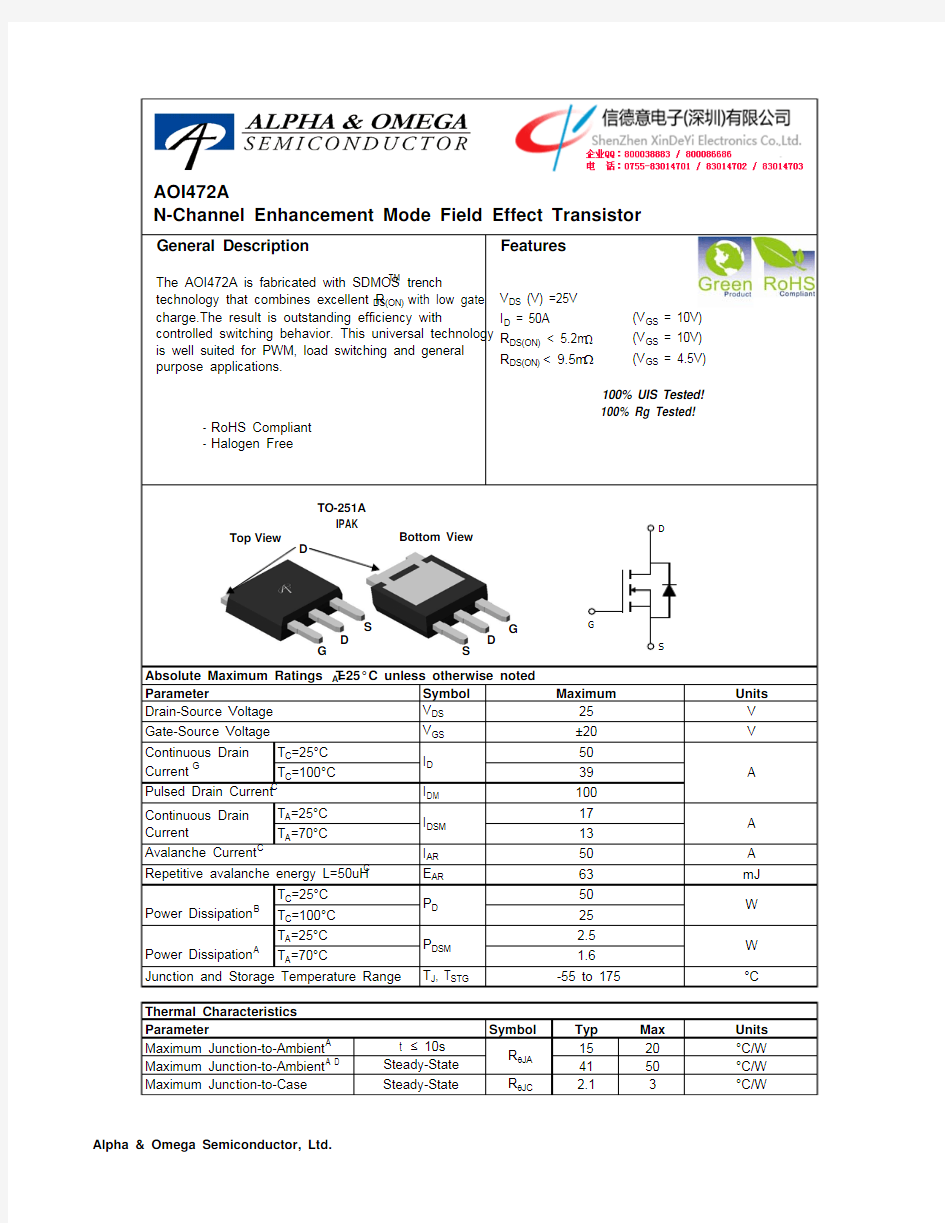
R θJA AOI472A
Absolute Maximum Ratings T A =25°C unless otherwise noted
Maximum Junction-to-Case
Steady-State
°C/W
Steady-State °C/W Maximum Junction-to-Ambient A D G
G
D
D
S
S
D
Top View
Symbol
Min Typ Max Units BV DSS 25
V
V DS =25V, V GS =0V
10T J =55°C
50I GSS 100
nA V GS(th)Gate Threshold Voltage 1.22
2.5
V I D(ON)
100
A 4.3
5.2T J =125°C
6.2
7.489.5
m ?g
FS 65S V SD 0.7
1V I S
50
A C iss 1500
18002200pF C oss 340445580pF C rss 200285400pF R g
1.1 1.6
2.4?Q g (10V)25
3140nC Q g (4.5V)121520nC Q gs 3.5 4.87nC Q gd 6.5
8.913nC t D(on)8ns t r 10.4ns t D(off)29ns t f 9
ns t rr 9.51215ns Q rr
17
21
26nC
Repetitive avalanche energy L=50uH C
Rev0 : Dec-08
COMPONENTS IN LIFE SUPPORT DEVICES OR SYSTEMS ARE NOT AUTHORIZED. AOS DOES NOT ASSUME ANY LIABILITY ARISING OUT OF SUCH APPLICATIONS OR USES OF ITS PRODUCTS. AOS RESERVES THE RIGHT TO IMPROVE PRODUCT DESIGN,FUNCTIONS AND RELIABILITY WITHOUT NOTICE.
Body Diode Reverse Recovery Charge I F =30A, dI/dt=500A/μs
Maximum Body-Diode Continuous Current
Input Capacitance Output Capacitance Turn-On DelayTime DYNAMIC PARAMETERS Turn-On Rise Time Turn-Off DelayTime V GS =10V, V DS =12.5V, R L =0.42?, R GEN =3?Gate resistance
V GS =0V, V DS =0V, f=1MHz
Turn-Off Fall Time
Total Gate Charge V GS =10V, V DS =12.5V, I D =30A
Gate Source Charge Gate Drain Charge Total Gate Charge m ?I S =1A,V GS =0V V DS =5V, I D =30A
V GS =4.5V, I D =20A
Forward Transconductance
Diode Forward Voltage R DS(ON)Static Drain-Source On-Resistance
I DSS μA V DS =V GS I D =250μA V DS =0V, V GS = ±20V Zero Gate Voltage Drain Current Gate-Body leakage current Electrical Characteristics (T J =25°C unless otherwise noted)STATIC PARAMETERS Parameter
Conditions Body Diode Reverse Recovery Time
Drain-Source Breakdown Voltage On state drain current
I D =250μA, V GS =0V V GS =10V, V DS =5V V GS =10V, I D =30A
Reverse Transfer Capacitance I F =30A, dI/dt=500A/μs
V GS =0V, V DS =12.5V, f=1MHz SWITCHING PARAMETERS A. The value of R θJA is measured with the device mounted on 1in 2
FR-4 board with 2oz. Copper, in a still air environment with T A =25°C. The Power dissipation P DSM is based on R θJA and the maximum allowed junction temperature of 150°C. The value in any given application depends on the user's specific board design, and the maximum temperature of 175°C may be used if the PCB allows it.
B. The power dissipation P D is based on T J(MAX)=175°C, using junction-to-case thermal resistance, and is more useful in setting the upper dissipation limit for cases where additional heatsinking is used.
C. Repetitive rating, pulse width limited by junction temperature T J(MAX)=175°C. Ratings are based on low frequency and duty cycles to keep initial T J =25°C.
D. The R θJA is the sum of the thermal impedence from junction to case R θJC and case to ambient.
E. The static characteristics in Figures 1 to 6 are obtained using <300μs pulses, duty cycle 0.5% max.
F. These curves are based on the junction-to-case thermal impedence which is measured with the device mounted to a large heatsink, assuming a maximum junction temperature of T J(MAX)=175°C. The SOA curve provides a single pulse rating.
G. The maximum current rating is limited by bond-wires.
H. These tests are performed with the device mounted on 1 in 2
FR-4 board with 2oz. Copper, in a still air environment with T A =25°C.
TYPICAL ELECTRICAL AND THERMAL CHARACTERISTICS
020
40
6080
1
2
3
4
5
V GS (Volts)
Figure 2: Transfer Characteristics (Note E)
I D (A )
02040
6080
100
1
2
3
4
5
V DS (Volts)
Fig 1: On-Region Characteristics (Note E)
I D (A )
TYPICAL ELECTRICAL AND THERMAL CHARACTERISTICS
02
4
6
8
10
5
10
1520253035
Q g (nC)
V G S (V o l t s )
0400
800120016002000240028000
5
10152025
V DS (Volts)
C a p a c i t a n c e (p F )
TYPICAL ELECTRICAL AND THERMAL CHARACTERISTICS
Vds
Charge
Gate Charge Test Circuit & Waveform
Resistive Switching Test Circuit & Waveforms
Vdd
Vds
Id
Vgs
BV I Unclamped Inductive Switching (UIS) Test Circuit & Waveforms
AR
DSS
2
E = 1/2 LI Vdd
AR AR