基于量子点元胞自动机纳米技术的超越CMOS下一代计算(IJEM-V8-N1-3)
I.J. Engineering and Manufacturing, 2018, 1, 25-37
Published Online January 2018 in MECS (https://www.360docs.net/doc/6712796290.html,)
DOI: 10.5815/ijem.2018.01.03
Available online at https://www.360docs.net/doc/6712796290.html,/ijem
An Insight into Beyond CMOS Next Generation Computing using Quantum-dot Cellular Automata Nanotechnology
Bisma Bilal a,b, Suhaib Ahmed a,*, Vipan Kakkar a
a Department of Electronics and Communication Engineering, Shri Mata Vaishno Devi University, Katra
182320, India
b Department of Electronics and Communciation Engineering, National Institute of Technology Srinagar,
Hazratbal 190006, India
Received: 08 June 2017; Accepted: 11 September 2017; Published: 08 January 2018
Abstract
CMOS is a technology that has revolutionized the field of electronics. Over the time the processing technologies and design methodologies of CMOS devices have proved to be in full swing with the Moore’s law and the miniaturization paradigm. However, after surviving for more than five decades, CMOS is now facing challenges to live through the submicron ranges. The scaling in CMOS has reached a higher limit, showing adverse effects not only from physical and technological point of view but also from material and economical perspective. This drift inspires the researchers to look for new promising alternatives to CMOS which vow better performance, density and power consumption. One of the promising alternatives to digital designing in CMOS is the Quantum-dot Cellular Automata (QCA). QCA is a technology that involves no current transfer but works on electronic interaction between the cells. The QCA cell basically consists of quantum dots separated by certain distance and the entire transmission of information occurs via the interaction between the electrons localized in these quantum dots. In this paper the limitations to CMOS in submicron range and concepts for designing in QCA have been discussed. Further the building blocks are explained theoretically as well as using QCA Designer implementations with focus on cell interaction and clocking mechanisms.
Index Terms: QCA, Quantum Dots, Quantum Cell, CMOS, Scaling, Clocking, Nanotechnology.
? 2018 Published by MECS Publisher. Selection and/or peer review under responsibility of the Research Association of Modern Education and Computer Science.
1.Introduction
The ever improving life of human beings is the direct result of the advancing technologies that are developed * Corresponding author.
E-mail address: sabatt@https://www.360docs.net/doc/6712796290.html,
from time to time. One of the most important contribution towards the improvement of human life is the development of the field of electronics which has by and large given a new scope to it. The major revolution that forms the core of the electronics industry today is the development of the CMOS technology. This technology has given a new dimension to computing over the last five decades. From 1947, when the first bipolar junction transistors were invented to the time when MOSFET’s took over the improvements were occurring at a pace that was not so fast. However after the development of CMOS, the paradigm of miniaturization has achieved much exhilaration and the scaling of CMOS completely met and satisfied this framework. The exceptional growth that the industry has seen over the last few decades has been due to the successful linear scaling which was proposed by Dennard et.al [7], in the basic MOS structure. The scaling of the basic device can be divided into two categories viz. the constant voltage scaling, in which the not so practical concept of scaling of voltage is taken into consideration and the constant field scaling, in which all the dimensions including the power supply voltages and the terminal voltages of the MOSFET are reduced by a same factor. Howbeit it was Moore, who in his paper [4] suggested that the number of components per integrated circuit would approximately double every two years without the corresponding increase in the cost of the chip. This meant that the growth would be exponential. From the time this was predicted by Moore, till toda y the industry has managed to keep up with the above fundamental famously known as the Moore’s Law. However as suggested by the International Technology and Roadmap for Semiconductors ITRS, the CMOS technology has now started to face asperities in maintaining the miniaturization criterion and holding on to the Moore’s law [1-3]. The immediate effect of the exponential growth is the ever increasing power dissipation on a single integrated circuit. As the number of components keeps on increasing the power dissipation goes on increasing given a constant power handling capability of the chip. The possibility of removing this generated heat from the chip becomes more and more difficult as the size of the devices goes down to the sub-micron ranges. This implies that the scaling of the basic MOS structure is now reaching the quantum limitations wherein the possibility of further scaling has started to lose its grounds. This is because of the size limitation which means that as the dimensions of the basic device are now approaching the atomic and molecular sizes the possibility of further scaling of the basic device is ruled out leaving no scope for downsizing of the devices [5, 6].
2.Limitations of CMOS Technology
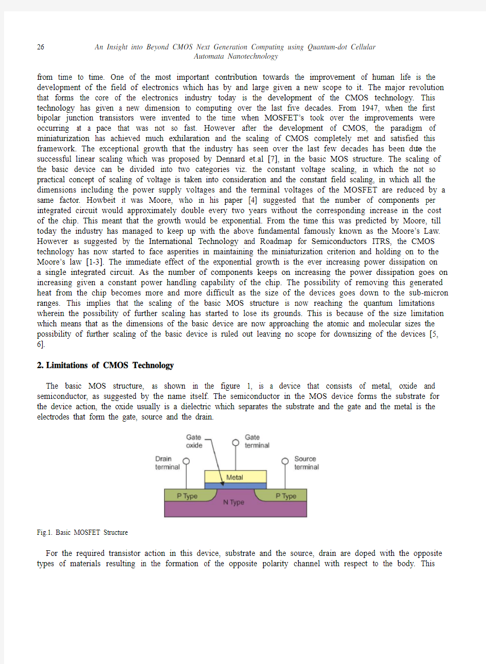
The basic MOS structure, as shown in the figure 1, is a device that consists of metal, oxide and semiconductor, as suggested by the name itself. The semiconductor in the MOS device forms the substrate for the device action, the oxide usually is a dielectric which separates the substrate and the gate and the metal is the electrodes that form the gate, source and the drain.
Fig.1. Basic MOSFET Structure
For the required transistor action in this device, substrate and the source, drain are doped with the opposite types of materials resulting in the formation of the opposite polarity channel with respect to the body. This
structure forms the basic MOS device. The basic parameters that determine the characteristics of the device include the voltage applied to the gate terminal called as the gate-source voltage, the voltage between the drain and the source called the drain source voltage, the capacitance offered by the oxide that is the oxide capacitance, the threshold voltage that is the minimum required voltage for formation of the channel and the current that flows between the source and the drain defined as the drain-source current.
As the dimensions of the device are scaled down to the nano meter regime, the parameters are affected by the various quantum effects which results in the degradation in the performance or even the failure of the device. The limitations that the technology is facing does not include a single dimension but has to be envisaged from multiple viewpoints which include the physical, technological, economic and the material perspectives [8]. When we consider the scaling effects, the first and the foremost is the physical effect of this scaling. As all the dimensions of the device are scaled by the same factor both channel length and thickness of the dielectric change. Due to the reduction in the length of the channel the various short channel effects come into the picture. They include the drain induced barrier lowering (DIBL) wherein the high reverse bias at the drain reduces the barrier faced by the carriers and allow the currents to flow for voltages less than the threshold voltage of the device [9]. On the other hand as the scaling diminishes the oxide thickness, it approaches to the width of just a few layers of molecules. Under these size considerations, the various quantum effects start dominating and the electrons start tunnelling through the oxide. Due to this the carriers become available for the voltages at which a normally operated device would not allow conduction. Besides these effects, the short channel of the device can also lead to merging of the source and the drain regions due to the reverse bias of the drain, thereby hampering the basic functioning of the device. To avoid these effects, the doping of the channel can be increased but that again shows adverse effects like the decrease in the mobility of the carriers and the band to band tunnelling. So the physical dimension forms the first aspect into which the limitations of CMOS are rooted.
Apart from the physical aspect, the material stance also plays an important part in not favoring the future scaling. Switching from one material to other in CMOS has not been much of interest to the researchers but now as the end of the technology roadmap is approaching the plunge into the ocean of materials to find a suitable case for CMOS can act as a savior. The technological perspective for the current devices has its life in the various lithographic techniques invented from time to time. However in the deca nanometer regime the conventional lithographic techniques can no longer cope up. So new technologies need to be investigated to give some more life to CMOS. The last but not the least is the economic outlook. The industry cannot go on without actually checking the cost to benefit ratios. We cannot design the components and devices with no returns. Besides, smaller the size more are the defects and the cost of overcoming them. So all these areas need to be studied in order to come up with some solutions to actually implement the concept of “more than moore” today [10, 11].
3.Upcoming Alternates to CMOS Technology
In order to continue with the miniaturization attribute, researches have pointed out two broad categories which include firstly, the development of the CMOS based devices that extend to 3D or vertical dimension and improving material technology etc. and secondly, the switching from the usual transistor paradigm to other phenomena of physics. In order to go with the first option new materials like strained Si or high K dielectrics and new structures like the multi-gate and SOI need to be studied to the extend where they can be used to replace the existing designs in a reasonable amount of time. On the other hand a shift from the transistor based paradigm is the new broad area of research that has been unfolded. It includes a number of alternatives such as the quantum computing, carbon nanotubes, resonant tunnelling devices, single electron devices and the Quantum-dot Cellular Automata Nanotechnology. All these emerging fields are attracting a lot of attention of the researchers since the life of CMOS somehow is to come to an end in a few decades. To obtain if not an alternative, a complement for CMOS, these areas and technologies have witnessed a huge research interest in
recent years [12-13].
4.Quantum-dot Cellular Automata (QCA)
One of the most promising technology as seen by the researchers is the nanotechnology based Quantum Cellular Automata [14]. This technology incorporates a shift from the conventional transistorized designs to designing using nano structures like quantum dots or metal islands. This archetype works on the principles of quantum physics and uses the effects that were a threat to CMOS to its advantage. This is a cellular type of a design as suggested by Von Neumann in his architectures. It was developed by C.S.Lent [14]. The basic QCA cell consists of four potential wells which can be made from quantum dots, metal islands or other nano structures, as shown in figure 2. These wells localize two electrons which tunnel between these due to the presence of tunnel junctions. This quantum mechanical tunnelling forms the first basic principle of QCA designing. The second principle is the most famous law of physics which is the coulomb’s law. The electrons in the wells experience a coulombic repulsion between them due to which the electrons in the square structure of the cell take up only two types of stable configurations. These configurations are called as the two types of polarizations of the cell, as shown in figure 2. They represent the binary zero and binary one for the digital designing using QCA. However in the QCA cells no tunnelling is allowed between the adjacent cells and hence there is no current flow in this technology. Here the interaction between the cells forms the basic mechanism of functioning. The cells which are adjacent to each other have the ability to effect the polarization of each other. Due to this the state of each cell depends on the state of the adjacent cell.
Fig.2. A basic QCA cell and Binary 1 and 0 polarization representations.
The QCA designing follows the phenomena of processing in the wire and memory in motion which means that the interconnections in this technology are not different from the circuits used [21,31,32]. The cell which is provided with the input effects the cell next to it and changes its polarization so as to achieve a stable state with least coulombic repulsions between them. In this way long wires called as binary wires can be designed in QCA. The majority gate and inverter form the other two most important components in QCA. All these components are shown in the figure 3.
(a)
(b) (c)
Fig.3. (a) Binary Wire, (b) Inverter and (c) 3-Input Majority Gate in QCA
The inverter is designed using the 45°cell at the corner in the design. Due to this shift of the cell, the least coulombic forces are experienced in the cell alignment with opposite polarization and hence an inverter. The majority gate, as the name suggests achieves a stable state depending on the value of the three inputs. In this gate the central cell called as the device cell takes up the polarization of the majority of inputs to achieve a stable state [15-16]. Just as in digital logic we have some basic circuits from which the entire digital circuitry can be designed, in QCA. Besides the design of basic Boolean functions the entire circuitry of a digital computer can be designed in QCA. For example, by fixing one of the input of the majority gate to zero, an OR gate can be designed. Similarly by fixing one input to one, an AND gate can be realized.
By combining these AND and OR gates with the inverter NAND and NOR logics can be achieved. Further by proper connections between the majority gates other Boolean functions can be realized. The basic designs of NAND and NOR gates are shown in figure 4.
(a) (b)
Fig.4. (a) NAND and (b) NOR Gate Implementation in QCA
The basic method of designing involves the conventional majority voter designing. Other than this a number of design methodologies have been suggested one of which is the designing based on the explicit interaction of cells [25,31,32] and the other is the tile based designs. All these designing methods are under research and a break through from these is expected, thus leading to the revolution from the transistor based designing to the no current paradigms. Some of the designs in QCA are discussed in the next section.
The proper flow of information in the QCA architectures is ensured by the clocking of the circuits which is provided by the underlining CMOS or carbon nanotube wires. The function of this clocking is to provide the electric field to the QCA cells which in turn controls the raising and lowering of the barriers between the wells. Due to the change in the barrier potential, the electrons in the wells are either localized or allowed to tunnel to
other well. If the barriers are lowered, the electrons tunnel from one well to another such that to ensure least coulombic repulsion with respect to the adjacent cells. On the other hand, if the barriers are raised, the electrons localize in a particular well and the tunnel junctions are closed to any movement of electrons. In QCA, one clock cycle consists of four phases. The phases decide whether the barriers are low or high. The first is the switch phase, in which the barriers are lowered and the electrons are allowed to respond to the effect of the adjacent cell. By the end of the switch phase, the electrons take up a particular polarization corresponding to the neighboring cell. The next phase is the hold phase, in which the barriers are raised and no movement of electrons occurs. In this case the cell is in the position to influence the adjacent cell. Depending on the clock phase of the next cell it may either remain in the same state (if this is also in hold state) or change its polarization (if it is in switch or release phase). The phase that follows the hold phase is the release and relax phase in which the barriers are again lowered and the cell again attains the null polarization. For proper working of the QCA circuits the clocking of the circuits in a proper manner is very important. The clock phases should follow each other in a proper manner otherwise the information flow can be distorted. Due to four phases, the QCA architecture is provided with four clock zones as shown the figure 5. The proper flow of information is also explained in figure 5. In QCA the different phases of a clock cycle are represented by different colors [29-31].
5.QCA Based Digital Design Implementations
In this section some basic designs in QCA have been discussed to get an idea about the flow of information via pipelining. As discussed earlier the binary wire, inverter and the majority gate form the basic building blocks in QCA. All the circuitry designed using QCA involves the use of these basic building block. We have already discussed the designs of basic Boolean functions. The digital circuitry however comprises of two broad categories of designs which are the combinational and the sequential logic. In conventional digital designing the clock is required only in sequential logic whereas in case of QCA designing clocking is required in both combinational and sequential logic designs [17-19,27,28,31]. The optimization parameters in this technology include the cell count of the design, latency, cell area, total area and complexity of the design. Here we have discussed some of the widely used combinational and sequential circuit designs and have also explained the basic working and clocking of the designs.
Fig.5. Clocking Zones and Phases Along with Illustration of Information Flow in QCA
The figure 6 shows the QCA implementation of a half adder along with the simulation results that have been achieved in the QCA Designer 2.0.3. From the equations of the half adder we know that we have a sum and a carry output, given by the equations Sum=A?B and Carry=AB. So we now need to implement these two equations in order to design a half adder in QCA. The majority equations can be written in order to simplify the design process. The majority equations for a half adder are given by
SUM=M(M(A,B′,?1),M(A′,B,?1),1) (1) CARRY=M(A,B,?1) (2) From the carry equation we see that it simply consists of a single majority gate in which one input is fixed to one in order to obtain an AND operation. The equation for sum is however more complicated as it involves the designing of an Exclusive-OR gate. The equation of the Exclusive-OR function is given by A′B?AB′. This means that the implementation of the Ex-OR function needs two inverters, two AND gates and one OR gate. This is implemented in the figure 6.
Fig.6. QCA Implementation of a Half Adder
Fig.7. Simulation Result of a Half Adder using QCA Designer 2.0.3
The other circuit is the full adder. This adder can be designed using the conventional majority voter method but here we have shown the design using the explicit interaction of cells. The implementation full adder in QCA Designer 2.0.3 is shown in figure 8.
Fig.8. QCA implementation of a full adder
Fig.9. Simulation Results of a full adder using QCA Designer 2.0.3
The sequential circuits are the other class of digital circuits which are the fundamental in the designing of complex computer architectures [20]. The basic sequential circuit is the flip flop. We have considered a basic D flip flop design. The D flip flop is basically a delay flip flop which means that one D flip flop provides a delay
of one [26]. We also know that in QCA one clock cycle consists of four phases and is equal to one delay. Hence a simple QCA wire which has all four phases of the clock can provide a delay of one and can hence act as a D flip flop. This is shown in figure 10.
Fig.10. QCA Implementation of D-Flip Flop
Fig.11. Simulation Results for D-Flip Flop using QCA Designer 2.0.3
The other sequential circuit we have considered is the four bit shift register. It consists of four D flip flops. After each clock cycle i.e. each D flip flop the bits are shifted. This is shown in figure 12.
Fig.12. 4 Bit Shift Register Using D Flip Flop
Fig.13. Simulation Results of Shift Register Using QCA Designer 2.0.3
Besides the combinational and sequential designing using QCA, a new emerging digital logic is finding wide scope in design using QCA technology. The logic is called as the reversible logic which suggests that the power is dissipated in the circuits due to the erasing of the bits during computation. This principle was given by Landauer. It suggests that for every bit that is erased KTln2 joules of energy is dissipated. If these computations are somehow performed in a reversible manner that is without the erasing of the bits the power dissipation can be reduced to a great extent [22-24]. However the design of the reversible circuits has been the greatest challenge faced by the researchers. QCA is suggested as the break through by which these circuits can be implemented. Reversible logic along with QCA technology if accomplished will result in ultra-small devices and ultra-low power dissipation.
6.Advantages of QCA
QCA stands as a strong contender as an alternative or complement to CMOS due to the numerous advantages it offers over the conventional CMOS technology. Some of the important advantages over CMOS involve the ultra-small size designs that are possible using this technology. The basic cell in QCA is only a few nanometers in size and thus the overall architectural area depends on the efficiency of the designs which are implemented. This results in the achievement of very high density circuits in QCA which cannot be possible with the present CMOS structures. QCA technology is an edge driven one which means that the input is to be applied to a single cell at the edge. The inner cells respond to the input cell and adjust their polarization. This also suggests that no power lines are required and the resulting architectures are therefore ultra low power designs. This is the most important advantage of QCA since this power dissipation is the main showstopper for the CMOS technology.
7.Conclusion
In this paper we have reviewed the CMOS technology and have discussed the various limitations that are forcing the CMOS towards the end of the technology roadmap. Further we have envisaged the future of the electronics industry in either improving CMOS materials and structures or shifting from the transistor based paradigms. We have focused on one of the promising upcoming alternative of CMOS which is the Quantum Dot Cellular Automata. We have discussed the basic building block in QCA and the fundamentals of the working of the QCA architectures via clocking and pipelining. The various examples to understand the basic designs are discussed and the advantages of QCA over CMOS are listed. We thus conclude that the shift from the transistor based paradigm may not take years but decades of effort but they are the need of the hour for nanotechnology and next generation computer architectures.
References
[1]Yong B. Kim, “Challenges for nanoscale MOSFETs and emerging nanoelectronics”, Transaction on
Electrical and Electronic Materials, vol. 11, no. 3, pp. 93–105, 2010.
[2]J. Gautier, “Beyond CMOS: quantum devices”, Microelectronic Engineering, Volume 39, no. 1–4,
December 1997, pp. 263-272.
[3]David Bishop, “Nanotechnology and end of Moore’s law”, Bell Labs Technical Journal, vol. 10, no. 3, pp.
23-28, 2005.
[4]G. E. Moore, “Cramming More Components Onto Integrated circuits”, Proceedings of the IEEE, vol. 86,
no.1, pp. 82–85.
[5]John M. Shalf; Robert Leland, “Computing beyond Moore's Law” Computer, vol. 48, no. 12, pp. 14 - 23,
2015.
[6]H. Iwai, “End of the scaling theory and Moore's law”, Proc. of 16th IEEE Int ernational Workshop on
Junction Technology, 2016, pp. 1-4.
[7]R.H. Dennard, F.H. Gaensslen, L. Kuhn, H.N. Yu, “Design of Micron MOS Switching Devices”, IEEE
Intl. Electron Devices Meeting, Dec 1972, pp. 344.
[8]Nor Zaida Haron, Said Hamdioui, “Why is CMOS scaling coming to an END?” IEEE 3rd International
Design and Test Workshop, 2008. IDT 2008.
[9]Hiroshi Iwai, “Materials and structures for future nano CMOS”, IEEE Conference on Nanotechnology
Materials and Devices (NMDC), 2011, pp.14-18
[10]E.J. Nowak, “Maintaining the benefits of CMOS scaling when scaling bogs down”, Journal of Research
and Development, pp.169-180, 2002
[11]S.G. Narenda, “Challenges and Design Choices in Nanoscale CMOS”, ACM Journal on Emerging
Technologies in Computing Systems, vo1, no.1 pp.7-49, 2005
[12]M ehdi Askari, Maryam Taghizadeh, Khossro Fardad “Digital design using quantum-dot cellular automata
(A nanotechnology method)”, IEEE International Conference on Computer and Communication
Engineering, ICCCE, pp. 952-955, 2008
[13]Mark Horowitz, “What’s next after CMOS”, IEEE Hot Chips 19 Symposium (HCS), 2007.
[14]C.S. Lent, P.D. Tougaw, W. Porod, G.H. Bernstein, “Quantum Cellular Automata,” Nanotechnology, Vol.
4, no.1, pp. 49–57, 1993
[15]Wolfgang Porod, “Quantum-dot devices and quantum-dot cellular automata”, Interna tional Journal of
Bifurcation and Chaos, vol. 7, no. 10, pp. 1147-1175, 1997.
[16]P.D. Tougaw, C.S. Lent, “Logical devices implemented using quantum cellular automata”, Journal of
Applied Physics , vol. 75, no. 3, pp. 1818-1825, 1994.
[17]Heumpil Cho, Earl E. Sw artzlander, “Adder and multiplier design in quantum-dot cellular automata”,
IEEE Transactions on Computers, vol. 58, no. 6, pp. 721-727 2009
[18]Keivan Navi, Razieh Farazkish, Samira Sayedsalehi, Mostafa Rahimi Azghadi, “A new quantum dot
cellular automata full-adder”, Microelectronics Journal, vol. 41, no. 12, pp. 820–826, 2010.
[19]Dariush Abedi, Ghassem Jaberipur, and Milad Sangsefidi, “Coplanar full adder in quantum-dot cellular
automata via clock-zone-based crossover”, IEEE Transactions on Nanotechnology, vo l. 14, no. 3, pp. 497-504, 2015
[20]Abbas Shahini Shamsabadi, Behrouz Shahgholi Ghahfarokhi, Kamran Zamanifar, Naser Movahedinia,
“Applying inherent capabilities of quantum-dot cellular automata to design: D flip-flop case study”, Journal of Systems Architecture, vol. 55, no. 3, pp.180-187, 2009.
[21]Michael Gladshtein, “Quantum-dot cellular automata serial decimal processing-in-wire: Run-time
reconfigurable wiring approach” Microelectronics Journal, vol. 55, pp. 152–161, 2016
[22]R. Landauer, “Irreversibility and Heat Generation in the Computing Process”, IBM Journal of Research
and Development, vol. 5, no. 3, pp. 183-191, 1961.
[23]C.H. Bennett, “Logical Reversibility of Computation”, IBM Journal of Research and Development, vol.
17, pp. 525-532, 1973
[24]R. Feynman, “Quantum Mechanical Computers,” Optical New, pp. 11- 20, 1985.
[25]Firdous Ahmad, Ghulam Bhat, Hossein Khademol hosseini, Saeid Azimi, Shaahin Angizi, Keivan Navi,
“Towards single layer quantum-dot cellular automata adders based on explicit interaction of cells”, Journal of Computational Science , vol. 16, pp. 8–15, 2016.
[26]M. R. Beigh, M. Mustafa, “Design and Analysis of a Simple D Flip-Flop Based Sequential Logic Circuits
for QCA Implementation”, IEEE Conference on Computing for Sustainable Global Development (INDIACom), 2014, pp. 536-540.
[27]A. Roohi, R. Zand, S. Angizi, and R. F. Demara, "A Parity-Preserving Reversible QCA Gate with Self-
Checking Cascadable Resiliency," IEEE Transactions on Emerging Topics in Computing, 2016.
[28]B. Sen, M. Dutta, and B. K. Sikdar, "Efficient design of parity preserving logic in quantum-dot cellular
automata targeting enhanced scalability in testing," Microelectronics Journal, vol. 45, pp. 239-248, 2014.
[29]A.O. Orlov, I. Amlani, R.K. Kummamuru, R. Ramasubramaniam, G. Toth, C.S. Lent, et al.,
"Experimental demonstration of clocked single-electron switching in quantum-dot cellular automata,"
Applied Physics Letters, vol. 77, pp. 295-297, 2000.
[30]A. O. Orlov, R. K. Kummamuru, R. Ramasubramaniam, G. Toth, C. S. Lent, G. H. Bernstein, et al.,
"Experimental demonstration of a latch in clocked quantum-dot cellular automata," Applied Physics Letters, vol. 78, pp. 1625-1627, 2001.
[31]B. Bilal, S. Ahmed, V. Kakkar, “Optimal Realization of Universality of Peres Gate using Explicit
Interaction of Cells in Quantum Dot Cellula r Automata Nanotechnology,” International Journal of Intelligent Systems and Applications, vol. 9, no. 6, pp. 75-84, 2017.
[32]B. Bilal, S. Ahmed, V. Kakkar, “QCA Based Efficient Toffoli Gate Design and Implementation for
Nanotechnology Applications,” Internat ional Journal of Engineering and Technology, vol. 9, no. 3s, pp.
84-92, 2017.
Authors’ Profiles
Bisma Bilal received her B.Tech degree in electronics and communication engineering from
Islamic University of Science and Technology, Jammu and Kashmir, India and completed the
M.Tech degree in electronics and communication engineering at Shri Mata Vaishno Devi
University, Katra, India in 2017. She is currently pursuing Ph.D. degree in electronics and
communication engineering from National Institute of Technology Srinagar. Her research
interests include Nanotechnology, Quantum Cellular Automata, analog and digital VLSI design and biomedical VLSI
Suhaib Ahmed was born in Jammu, India, in 1991. He received the B.E. degree in electronics
and communication engineering from University of Jammu, India, in 2012 and M.Tech. degree
in electronics and communication engineering from Shri Mata Vaishno Devi University, India,
in 2014. He is currently pursuing his Ph.D. degree in electronics and communication
engineering from Shri Mata Vaishno Devi University, India.
His research interests include nanotechnology, QCA, energy harvesting, implantable microsystems, application of wireless sensor networks in health and environment monitoring and biomedical systems. He is currently working on design and modeling of ultra low power mixed signal circuits for implantable devices.
Mr. Ahmed is a member of IEEE, International Association of Engineers and Associate Member of Universal Association of Computer and Electronics Engineers.
Vipan Kakkar was born in Amritsar, India, in 1973. He received the B.E. degree in
electronics and communication engineering from Nagpur University, India, in 1994 and M.S.
degree from Bradford University, UK, in 1997. He received his Ph.D. degree in electronics and
communication engineering from Delft University of Technology, Netherlands in 2002.
He worked in Research & Development at Phillips, Netherlands as engineer and system
architect from 2001 to 2009. Since 2009, he has been an Associate Professor with the Department of Electronics and Communication Engineering, Shri Mata Vaishno Devi University, Katra, India. His research interests include ultra low power analog and mixed signal design, MEMS design, synthesis and optimization of digital circuits, biomedical system and implants design, audio and video processing.
Dr. Kakkar is a Senior Member IEEE and Life Member IETE and has served as an Executive Member of IEEE and has published many research papers in International Conferences and peer reviewed journals. He has also authored a book on System on Chip Design and has served as an editorial board member of microelectronics and solid state electronics journal
How to cite this paper: Bisma Bilal, Suhaib Ahmed, Vipan Kakkar,"An Insight into Beyond CMOS Next Generation Computing using Quantum-dot Cellular Automata Nanotechnology", International Journal of Engineering and Manufacturing(IJEM), Vol.8, No.1, pp.25-37, 2018.DOI: 10.5815/ijem.2018.01.03
交通流中的NaSch模型及MATLAB代码元胞自动机完整
元胞自动机NaSch模型及其MATLAB代码 作业要求 根据前面的介绍,对NaSch模型编程并进行数值模拟: ●模型参数取值:Lroad=1000,p=,Vmax=5。 ●边界条件:周期性边界。 ●数据统计:扔掉前50000个时间步,对后50000个时间步进行统计,需给出的 结果。 ●基本图(流量-密度关系):需整个密度范围内的。 ●时空图(横坐标为空间,纵坐标为时间,密度和文献中时空图保持一致, 画 500个时间步即可)。 ●指出NaSch模型的创新之处,找出NaSch模型的不足,并给出自己的改进思 路。 ●? 流量计算方法: 密度=车辆数/路长; 流量flux=density×V_ave。 在道路的某处设置虚拟探测计算统计时间T内通过的车辆数N; 流量flux=N/T。 ●? 在计算过程中可都使用无量纲的变量。 1、NaSch模型的介绍 作为对184号规则的推广,Nagel和Schreckberg在1992年提出了一个模拟车辆交通的元胞自动机模型,即NaSch模型(也有人称它为NaSch模型)。 ●时间、空间和车辆速度都被整数离散化。
● 道路被划分为等距离的离散的格子,即元胞。 ● 每个元胞或者是空的,或者被一辆车所占据。 ● 车辆的速度可以在(0~Vmax )之间取值。 2、NaSch 模型运行规则 在时刻t 到时刻t+1的过程中按照下面的规则进行更新: (1)加速:),1min(max v v v n n +→ 规则(1)反映了司机倾向于以尽可能大的速度行驶的特点。 (2)减速:),min(n n n d v v → 规则(2)确保车辆不会与前车发生碰撞。 (3)随机慢化: 以随机概率p 进行慢化,令:)0, 1-min(n n v v → 规则(3)引入随机慢化来体现驾驶员的行为差异,这样既可以反映随机加速行为,又可以反映减速过程中的过度反应行为。这一规则也是堵塞自发产生的至关重要因素。 (4)位置更新:n n n v x v +→ ,车辆按照更新后的速度向前运动。 其中n v ,n x 分别表示第n 辆车位置和速度;l (l ≥1)为车辆长度;11--=+n n n x x d 表示n 车和前车n+1之间空的元胞数;p 表示随机慢化概率;max v 为最大速度。 3、NaSch 模型实例 根据题目要求,模型参数取值:L=1000,p=,Vmax=5,用matlab 软件进行编程,扔掉前11000个时间步,统计了之后500个时间步数据,得到如下基本图和时空图。 程序简介 初始化:在路段上,随机分配200个车辆,且随机速度为1-5之间。 图是程序的运行图,图中,白色表示有车,黑色是元胞。
元胞自动机简史
元胞自动机简史 元胞自动机的诞生是人类探索人的认识本质的结果,也是计算技术巨大进步推动的结果。自古以来,人类认识一般问题的根本方法就是,建模和计算(推演)。模型是人类智力能理解自然世界的唯一方式。而元胞自动机正是一种可以用来建模也非常容易进行计算的理论框架和模型工具。最早从计算的视角审视问题的是关心人的认识本质的哲学家。笛卡尔认为, 人的理解就是形成和操作恰当的表述方式。洛克认为, 我们对世界的认识都要经过观念这个中介, 思维事实上不过是人类大脑对这些观念进行组合或分解的过程。霍布斯更是明确提出, 推理的本质就是计算。莱布尼兹也认为, 一切思维都可以看作是符号的形式操作的过程。进入20 世纪, 弗雷格, 怀特海、罗素等人通过数理逻辑把人类的思维进一步形式化, 形成了所谓的命题逻辑及一阶和高阶逻辑。在他们看来, 逻辑和数学, 都是根据特定的纯句法规则运作的。在这里, 所有的意义都被清除出去而不予考虑。在弗雷格和罗素的基础上, 维特根斯坦在他的早期哲学中把哲学史上自笛卡尔以来的原子论的理性主义传统发展到了一个新的高度。在维特根斯坦看来, 世界是逻辑上独立的原子事实的总和, 而不是事物的总和; 原子事实是一些客体的结合, 这些事实和它们的逻辑关系都在心灵中得到表达: 我们在心灵中为自己建造了事实的形象。人工智能事实上就是试图在机器中实现这种理性主义理想的一门学科。 在计算理论发展过程中, 阿兰·图灵(A. Turing) 的思想可以说是最关键的。在1936 年发表的论文中, 图灵提出了著名的图灵机概念。图灵机的核心部分有三: 一条带子、一个读写头、一个控制装置。带子分成许多小格, 每小格存一位数; 读写头受制于控制装置, 以一小格为移动量相对于带子左右移动, 或读小格内的数, 或写符号于其上。可以把程序和数据都以数码的形式存储在带子上。这就是“通用图灵机”原理。图灵在不考虑硬件的前提下, 严格描述了计算机的逻辑构造。这个理论不仅解决了纯数学基础理论问题, 而且从理论上证明了研制通用数字计算机的可行性。 图灵认为, 人的大脑应当被看作是一台离散态机器。尽管大脑的物质组成与计算机的物质组成完全不同, 但它们的本质则是相同。。离散态机器的行为原则上能够被写在一张行为表上, 因此与思想有关的大脑的每个特征也可以被写在一张行为表上, 从而能被一台计算机所仿效。1950 年, 图灵发表了《计算机器和智能》的论文, 对智能问题从行为主义的角度给出了定义, 设计出著名的“图灵测验,论证了心灵的计算本质, 并反驳了反对机器能够思维的9 种可能的意见。 与图灵提出人的大脑是一台离散态的计算机的思想几乎同一时期, 计算机科学的另一个 开创者冯·诺伊曼(J . von Neumann) 则开始从计算的视角思考生命的本质问题。一个人工的机器能够繁殖它自己吗? 当年笛卡尔在声称动物是机器的时候, 就曾被这个问题所难住。但冯·诺伊曼要回答这个问题, 他要找到自动机产生后代的条件, 他要证明机器可以繁殖! 为此, 冯·诺伊曼作了一个思想实验。他想象一台机器漂浮在一个池塘的上面, 这个池塘里有许多机器的零部件。这台机器是一台通用的建造器: 只要给出任何一台机器的描述,这台机器就会在池塘中寻找合适的部件, 然后再制造出这台机器。如果能够给出它自身的描述, 它就可以创造出它本身。不过, 这还不是完全的自我繁殖, 因为后代机器还没有对自身的描述, 它们因此不能复制自己。所以, 冯·诺伊曼继续假定最初的机器还必须包含一个描述复制器, 一旦后代机器产生出来, 它也从亲代那里复制一份关于自身的描述, 这样, 后代机器就可以无穷无尽地繁殖下去。 冯·诺伊曼的试验揭示了一个深刻的问题:任何自我繁殖的系统的基因材料, 无论是自然的还是人工的, 都必须具有两个不同的基本功能: 一方面它必须起到计算机程序的作用, 是一种在繁殖下一代时能够运行的算法, 另一方面它必须起到被动数据的作用, 是一个能够复制和传给下一代的描述。1953 年沃森和克里克揭示的DNA 结构和自我复制的机理。DNA 的特性正好具备冯·诺伊曼所指出的两个要求。 然而, 冯·诺伊曼对他自己的动力学模型并不十分满意。他不能充分地获得最小的逻辑前提, 因为该模型仍然以具体的原材料的吸收为前提。冯·诺伊曼感到, 该模型没有很好地把过程的
基于元胞自动机模型的城市历史文化街区的仿真
文章编号: 1673 9965(2009)01 079 05 基于元胞自动机模型的城市历史文化街区的仿真* 杨大伟1,2,黄薇3,段汉明4 (1.西安工业大学建筑工程系,西安710032;2.西安建筑科技大学建筑学院,西安710055; 3.陕西师范大学历史文化学院,西安710061; 4.西北大学城市与资源学系,西安710069) 摘 要: 为了探讨当前城市规划中远期预测的科学性和准确性问题,将自组织理论与元胞自动机模型结合,在一定的时空区域,构建了一个城市增长仿真模型.将元胞自动机模型应用于西安市最具历史文化特色的区域中,形成自下而上的规划模型.元胞自动机模型对于西安回民区的空间发展城市历史文化特色街区的模拟具有一定的原真性和时效性,在时空中能反应当前的空间格局.元胞自动机在城市规划的预测中具有图式与范式结合的特点,在中长期的预测中形成符合城市规划发展战略的空间格局. 关键词: 元胞自动机;自组织;历史文化特色街区;空间演化 中图号: T U984 文献标志码: A 自组织理论是当前城市复杂性研究的主要研究方向之一.自组织是相对他组织而言,即自我、本身自主地组织化、有机化,意味着一种自动的、自发性的行为,一种自下而上、由内至外的发展方式.其主要涵义可以简单概括:在大多数情况下,作用于系统的外部力量并不能直接对系统的行为产生作用,而是作为一种诱因,即引入序参量引发系统内部发生相变,系统通过这一系列的变化自发地组织起来,最终大量微观个体的随机过程表现出宏观有序的现象[1]. 20世纪40年代U lam提出元胞自动机模型(Cellular Autom at o n M odel,CA),V on N eu m ann将其用于研究自复制系统的逻辑特性,且很快用于研究自组织系统的演变过程,其中对城市系统自组织过程的模拟是焦点问题[2 9]. CA是定义在一个具有离散状态的单元(细胞)组成的离散空间上,按一定的局部规则在离散时间维演化的动力学系统.一个CA模型通常包括单元、状态、邻近范围和转换规则4要素[9],单元是其最小单位,而状态则是单元的主要属性.根据转换规则,单元可以从一个状态转换为另外一个状态,转换规则通过多重控制函数来实现. 自组织理论的提出,对于解释相对封闭,具有自身演化规律的复杂适应系统中的复杂现象和问题具有重要意义和应用前景.而CA 自下而上的研究思路,强大的复杂计算功能、固有的并行计算能力、高度动态特征以及具有空间概念等特征,使其在模拟空间复杂系统的时空演变方面具有很强的能力,在城市学研究中具有天然优势[9 15].本文将自组织理论引入CA模型,并将该模型首次应用于西安回民区这一复杂的相对独立的历史街区中,就是为了得出其在自组织的作用下,未来20年空间发展的变化模型,为城市规划的制定做出科学的预测.下面对西安回民区做一简单介绍. 西安回民区位于西安旧城中心的中西地段,东接西安历史文化遗产钟楼和北大街,西接洒金桥,南到西大街,北到莲湖路,面积约为93.4公顷,人口约为77600人,在此居住的居民中有43.6%以 第29卷第1期 西 安 工 业 大 学 学 报 V o l.29No.1 2009年02月 Jo urnal o f Xi!an T echnolo g ical U niver sity Feb.2009 *收稿日期:2008 06 04 基金资助:国家自然科学基金(50678149) 作者简介:杨大伟(1981 ),男,西安工业大学助教,西安建筑科技大学博士研究生,主要研究方向为城市空间复杂性. E mail:yangdaw ei@https://www.360docs.net/doc/6712796290.html,.
CA元胞自动机优化模型原代码
CA优化模型原代码: M=load(‘d:\ca\jlwm’) N=load(‘d:\ca\jlwn.asc’) lindishy=load(‘d:\ca\ldfj3.asc’) caodishy=load(‘d:\ca\cdfj3.asc’) gengdishy=load(‘d:\ca\htfj3.asc’) [m,n]=size(M); Xr=[1 1 -1 1 1 1 -1 -1 1 1;1 1 1 1 -1 -1 1 1 1 -1;-1 1 1 1 -1 -1 -1 1 -1 -1;1 1 1 1 1 1 -1 1 1 I; l -1 -1 1 1 -1 -1 -1 1 1;1 -1 -1 1 -1 1 -1 1 -1 -1;-1 1 -1 -1 -1 -1 1 -1 -1 -1;-1 1 1 1 -1 1 -1 1 -1 -1;1 1 -1 1 1 -1 -1 -1 1 1;1 -1 -1 1 1 -1 -1 -1 1 1]; caodi=0;lindi=0;gengdi=0; for i=1:m forj=l:n if M(i,j)==4 caodi=caodi+1; elseif M(i,j)==3 lindi=lindi+1; elseif M(i,j)==2 gengdi=gengdi+1; end end end for i=1:m for j=1:n if M(i,j)==4 if lindishy(i,j)>gengdishy(i,j) if lindishy(i,j)>caodishy(i,j) z=0; for P=max(1,i-1):min(i+1,m) for q=max(j-1,1):min(j+1,n) if (M(p,q)~=0)&&xr(M(p,q),3)==-1 z=1; end end end if z== 0 caodi=eaodi-1; M(i,j)=3; lindi=lindi+1; end elseif lindishy(i,j)==caodishy(i,j) caoditemp=0; linditemp=0; gengditemp=0;
元胞自动机简史
元胞自动机简史元胞自动机的诞生是人类探索人的认识本质的结果,也是计算技术巨大进步推动的结果。自古以来,人类认识一般问题的根本方法就是,建模和计算(推演)。模型是人类智力能理解自然世界的唯一方式。而元胞自动机正是一种可以用来建模也非常容易进行计算的理论框架和模型工具。最早从计算的视角审视问题的是关心人的认识本质的哲学家。笛卡尔认为, 人的理解就是形成 和操作恰当的表述方式。洛克认为, 我们对世界的认识都要经过观念这个中介, 思维事实上不过是 人类大脑对这些观念进行组合或分解的过程。霍布斯更是明确提出, 推理的本质就是计算。莱布尼兹也认为, 一切思维都可以看作是符号的形式操作的过程。进入20 世纪, 弗雷格, 怀特海、罗素等人通过数理逻辑把人类的思维进一步形式化, 形成了所谓的命题逻辑及一阶和高阶逻辑。在他们看来, 逻辑和数学, 都是根据特定的纯句法规则运作的。在这里, 所有的意义都被清除出去而不 予考虑。在弗雷格和罗素的基础上, 维特根斯坦在他的早期哲学中把哲学史上自笛卡尔以来的原 子论的理性主义传统发展到了一个新的高度。在维特根斯坦看来, 世界是逻辑上独立的原子事实 的总和, 而不是事物的总和; 原子事实是一些客体的结合, 这些事实和它们的逻辑关系都在心灵中得到表达: 我们在心灵中为自己建造了事实的形象。人工智能事实上就是试图在机器中实现这种理性主义理想的一门学科。 在计算理论发展过程中,阿兰图灵(A. Turing)的思想可以说是最关键的。在1936年发表的论 文中, 图灵提出了著名的图灵机概念。图灵机的核心部分有三: 一条带子、一个读写头、一个控制装置。带子分成许多小格, 每小格存一位数; 读写头受制于控制装置, 以一小格为移动量相对于带子左右移动, 或读小格内的数, 或写符号于其上。可以把程序和数据都以数码的形式存储在带子上。这就是“通用图灵机”原理。图灵在不考虑硬件的前提下, 严格描述了计算机的逻辑构造。这个理论不仅解决了纯数学基础理论问题, 而且从理论上证明了研制通用数字计算机的可行性。 图灵认为, 人的大脑应当被看作是一台离散态机器。尽管大脑的物质组成与计算机的物质组成完全不同, 但它们的本质则是相同。。离散态机器的行为原则上能够被写在一张行为表上, 因此与思想有关的大脑的每个特征也可以被写在一张行为表上, 从而能被一台计算机所仿效。1950 年, 图灵发表了《计算机器和智能》的论文, 对智能问题从行为主义的角度给出了定义, 设计出著名的“图灵测验,论证了心灵的计算本质, 并反驳了反对机器能够思维的9 种可能的意见。 与图灵提出人的大脑是一台离散态的计算机的思想几乎同一时期, 计算机科学的另一个 开创者冯诺伊曼J . von Neumann)则开始从计算的视角思考生命的本质问题。一个人工的机器能 够繁殖它自己吗?当年笛卡尔在声称动物是机器的时候,就曾被这个问题所难住。但冯诺伊曼要回答这个问题, 他要找到自动机产生后代的条件, 他要证明机器可以繁殖! 为此,冯诺伊曼作了一个思想实验。他想象一台机器漂浮在一个池塘的上面,这个池塘里有许多机器的零部件。这台机器是一台通用的建造器: 只要给出任何一台机器的描述,这台机器就会在 池塘中寻找合适的部件, 然后再制造出这台机器。如果能够给出它自身的描述, 它就可以创造出它本身。不过, 这还不是完全的自我繁殖, 因为后代机器还没有对自身的描述, 它们因此不能复制自己。所以,冯诺伊曼继续假定最初的机器还必须包含一个描述复制器,一旦后代机器产生岀来,它也从亲代那里复制一份关于自身的描述, 这样, 后代机器就可以无穷无尽地繁殖下去。 冯诺伊曼的试验揭示了一个深刻的问题:任何自我繁殖的系统的基因材料,无论是自然的还是人工的, 都必须具有两个不同的基本功能: 一方面它必须起到计算机程序的作用, 是一种在繁殖下一代时能够运行的算法, 另一方面它必须起到被动数据的作用, 是一个能够复制和传给下一代的描述。1953 年沃森和克里克揭示的DNA 结构和自我复制的机理。DNA 的特性正好具备冯诺伊曼所指岀的两个要求。 然而, 冯诺伊曼对他自己的动力学模型并不十分满意。他不能充分地获得最小的逻辑前提, 因为该模型仍然以具体的原材料的吸收为前提。冯诺伊曼感到, 该模型没有很好地把过程的 逻辑形式和过程的物质结构区分开。作为一个数学家,冯诺伊曼需要的是完全形式化的抽象理
交通流元胞自动机模型综述
第23卷 第1期2006年1月 公 路 交 通 科 技 Journal of Highway and Transportation Research and Development Vol .23 No .1 Jan .2006 文章编号:1002-0268(2006)01-0110-05 收稿日期:2004-09-27 作者简介:郑英力(1971-),女,福建宁德人,讲师,研究方向为交通控制与仿真.(z hengyl71@s ina .com ) 交通流元胞自动机模型综述 郑英力,翟润平,马社强 (中国人民公安大学 交通管理工程系,北京 102623) 摘要:随着交通流模拟的需要及智能交通系统的发展,出现了基于元胞自动机理论的交通流模型。交通流元胞自动机模型由一系列车辆运动应遵守的运动规则和交通规则组成,并且包含驾驶行为、外界干扰等随机变化规则。文章介绍了交通流元胞自动机模型的产生与发展,总结和评述了国内外各种元胞自动机模型,并对元胞自动机模型的发展提出展望。 关键词:元胞自动机;交通流;微观模拟;模型中图分类号:U491.1+23 文献标识码:A Survey of Cellular Automata Model of Traffic Flow ZH ENG Ying -li ,ZH AI Run -p ing ,MA She -q iang (Department of Traffic Management Engineering ,Chinese People 's Public Security University ,Beijing 102623,China )Abstract :With the increas ing demand of traffic flow si mulation and the development of ITS research ,the traffic flow model based on cellular automata has been developed .Cellular automata model of traffic flow incorporates a series of vehicle movement rules and traffic regulations .Meanwhile ,the model works under some stochastic rules takin g into consideration of drivers 'behaviors and ambient interfer -ences .This paper introduces the establishment and development of cellular automata model of traffic flow ,su mmarizes and comments on different kinds of typical cellular automata models of traffic flow ,and furthermore ,presents a new perspective for further stud y of the model . Key words :Cellular automata ;Traffic flow ;Microscopic simulation ;Model 0 引言 交通流理论是运用物理学和数学定律来描述交通特性的理论。经典的交通流模型主要有概率统计模 型、车辆跟驰模型、流体动力学模型、车辆排队模型等 [1] 。20世纪90年代,随着交通流模拟的需要及智 能交通系统的发展,人们开始尝试将物理学中的元胞自动机(Cellular Automata ,简称CA )理论应用到交通领域,出现了交通流元胞自动机模型。 交通流C A 模型的主要优点是:(1)模型简单,特别易于在计算机上实现。在建立模型时,将路段分 为若干个长度为L 的元胞,一个元胞对应一辆或几辆汽车,或是几个元胞对应一辆汽车,每个元胞的状态或空或是其容纳车辆的速度,每辆车都同时按照所建立的规则运动。这些规则由车辆运动应遵守的运动规则和交通规则组成,并且包含驾驶行为、外界干扰等随机变化规则。(2)能够再现各种复杂的交通现象,反映交通流特性。在模拟过程中人们通过考察元胞状态的变化,不仅可以得到每一辆车在任意时刻的速度、位移以及车头时距等参数,描述交通流的微观特性,还可以得到平均速度、密度、流量等参数,呈现交通流的宏观特性。
元胞自动机NaSch模型及其MATLAB代码
元胞自动机N a S c h模型 及其M A T L A B代码 This manuscript was revised by the office on December 22, 2012
元胞自动机N a S c h模型及其M A T L A B代码 作业要求 根据前面的介绍,对NaSch模型编程并进行数值模拟: 模型参数取值:Lroad=1000,p=0.3,Vmax=5。 边界条件:周期性边界。 数据统计:扔掉前50000个时间步,对后50000个时间步进行统计,需给出的结果。 基本图(流量-密度关系):需整个密度范围内的。 时空图(横坐标为空间,纵坐标为时间,密度和文献中时空图保持一致,画500个时间步即可)。 指出NaSch模型的创新之处,找出NaSch模型的不足,并给出自己的改进思路。 流量计算方法: 密度=车辆数/路长; 流量flux=density×V_ave。 在道路的某处设置虚拟探测计算统计时间T内通过的车辆数N; 流量flux=N/T。 在计算过程中可都使用无量纲的变量。 1、NaSch模型的介绍 作为对184号规则的推广,Nagel和Schreckberg在1992年提出了一个模拟车辆交通的元胞自动机模型,即NaSch模型(也有人称它为NaSch模型)。 时间、空间和车辆速度都被整数离散化。道路被划分为等距离的离散的格子,即元胞。 每个元胞或者是空的,或者被一辆车所占据。 车辆的速度可以在(0~Vmax)之间取值。 2、NaSch模型运行规则 在时刻t到时刻t+1的过程中按照下面的规则进行更新: (1)加速:vnmin(vn1,vmax) 规则(1)反映了司机倾向于以尽可能大的速度行驶的特点。 (2)减速:vnmin(vn,dn) 规则(2)确保车辆不会与前车发生碰撞。 (3)随机慢化:以随机概率p进行慢化,令:vnmin(vn-1,0) 规则(3)引入随机慢化来体现驾驶员的行为差异,这样既可以反映随机加速行为,又可以反映减速过程中的过度反应行为。这一规则也是堵塞自发产生的至关重要因素。 (4)位置更新:vnxnvn,车辆按照更新后的速度向前运动。其中vn,xn分别表示第n辆车位置和速度;l(l≥1)为车辆长度; p表示随机慢化概率;dnxn1xn1表示n车和前车n+1之间空的元胞数; vmax为最大速度。 3、NaSch模型实例
元胞自动机理论基础
元胞自动机理论基础 Chapter1 元胞自动机(Cellular Automata,简称CA,也有人译为细胞自动机、点格自动机、分子自动机或单元自动机)。是一时间和空间都离散的动力系统。散布在规则格网 (Lattice Grid)中的每一元胞(Cell)取有限的离散状态,遵循同样的作用规则,依据确定的局部规则作同步更新。大量元胞通过简单的相互作用而构成动态系统的演化。不同于一般的动力学模型,元胞自动机不是由严格定义的物理方程或函数确定,而是用一系列模型构造的规则构成。凡是满足这些规则的模型都可以算作是元胞自动机模型。因此,元胞自动机是一类模型的总称,或者说是一个方法框架。其特点是时间、空间、状态都离散,每个变量只取有限多个状态,且其状态改变的规则在时间和空间上都是局部的。 1. 自动机 自动机(Automaton)通常指不需要人们逐步进行操作指导的设备(夏培肃,1984)。例如,全自动洗衣机可按照预先安排好的操作步骤作自动地运行;现代计算机能自动地响应人工编制的各种编码指令。完成各种复杂的分析与计算;机器人则将自动控制系统和人工智能结合,实现类人的一系列活动。另一方面,自动机也可被看作为一种离散数字动态系统的数学模型。例如,英国数学家A.M.Turing于1936年提出的图灵机就是一个描述计算过程的数学模型(TuringA M.,1936)。它是由一个有限控制器、一条无限长存储带和一个读写头构成的抽象的机器,并可执行如下操作: ·读写头在存储带上向左移动一格; ·读写头在存储带上向右移动一格; ·在存储的某一格内写下或清除一符号; ·条件转移。 图灵机在理论上能模拟现代数字计算机的一切运算,可视为现代数字计算机的数学模型。实际上,一切"可计算"函数都等价于图灵机可计算函数,而图灵机可计算函数类又等价于一般递归函数类。 根据存储带是否有限,可将自动机划分为有限带自动机(Finite Automaton)和无限带自动机(Infinite Automaton)。由于图灵机有无限长的存储带,所以为一种无限带自动机。有限带自动机常用作数字电路的数学模型,也用来描述神经系统和算法;而无限带自动机主要用来描述算法,也用来描述繁殖过程 (如细胞型自动机和网络型自动机)。 有限自动机是一种控制状态有限、符号集有限的自动机,是一种离散输入输出系统的数学模型。可将有限自动机设想成由一条划分为许多方格的输入带和一个控制器组成的机器:在输入带的每一个小格中可以容 纳一个符号,这些符号取自一个有限符号集S-控制器具有有限个可能状态(构成集合Q)。并在每一时刻仅处于其中的一个状态q;控制器有一个读入头,可以从输入带中读入符号;时间是离散的,初始时控制器处在状态;控制器的功能是根据其当前状态g和读入头从输入带上得到的符号a,来确定控制器的下一时刻的状态实现从状态q到状态q',实现从状态q到状态铲q'的转移,并将读入头右移一格。控制器另一功能是识别终止状态(它们构成Q的一个子集F),也可将该识别功能视为有限自动机的输出。 从数学上来定义,有限自动机是一个五元组: FA=(Q,S,δ,q0,F) 其中,Q是控制器的有限状态集、S是输入符号约有限集、δ是控制状态转移规律的Q×S到Q的映射(可用状态转移图或状态转移表表示),q0是初始状态、F是终止状态集。若δ是单值映射,则称M为确定性有限自动机;若δ是多值映射,则称M为非确定性有限自动机。
基于元胞自动机原理的微观交通仿真模型
2005年5月重庆大学学报(自然科学版)May2005第28卷第5期Journal of Chongqing University(Natural Science Editi on)Vol.28 No.5 文章编号:1000-582X(2005)05-0086-04 基于元胞自动机原理的微观交通仿真模型3 孙 跃,余 嘉,胡友强,莫智锋 (重庆大学自动化学院,重庆 400030) 摘 要:描述了一种对高速路上的交通流仿真和预测的模型。该模型应用了元胞自动机原理对复杂的交通行为进行建模。这种基于元胞自动机的方法是将模拟的道路量离散为均匀的格子,时间也采用离散量,并采用有限的数字集。同时,在每个时间步长,每个格子通过车辆跟新算法来变换状态,车辆根据自定义的规则确定移动格子的数量。该方法使得在计算机上进行仿真运算更为可行。同时建立了跟车模型、车道变换的超车模型,并根据流程对新建的VP算法绘出时空图。提出了一个设想:将具备自学习的神经网络和仿真系统相结合,再根据安装在高速路上的传感器所获得的统计数据,系统能对几分钟以后的交通状态进行预测。 关键词:元胞自动机;交通仿真;数学模型 中图分类号:TP15;TP391.9文献标识码:A 1 元胞自动机 生物体的发育过程本质上是单细胞的自我复制过程,50年代初,计算机创始人著名数学家冯?诺依曼(Von Neu mann)曾希望通过特定的程序在计算机上实现类似于生物体发育中细胞的自我复制[1],为了避免当时电子管计算机技术的限制,提出了一个简单的模式。把一个长方形平面分成若干个网格,每一个格点表示一个细胞或系统的基元,它们的状态赋值为0或1,在网格中用空格或实格表示,在事先设定的规则下,细胞或基元的演化就用网格中的空格与实格的变动来描述。这样的模型就是元胞自动机(cellular aut omata)。 80年代,元胞自动机以其简单的模型方便地复制出复杂的现象或动态演化过程中的吸引子、自组织和混沌现象而引起了物理学家、计算机科学家对元胞自动机模型的极大兴趣[1]。一般来说,复杂系统由许多基本单元组成,当这些子系统或基元相互作用时,主要是邻近基元之间的相互作用,一个基元的状态演化受周围少数几个基元状态的影响。在相应的空间尺度上,基元间的相互作用往往是比较简单的确定性过程。用元胞自动机来模拟一个复杂系统时,时间被分成一系列离散的瞬间,空间被分成一种规则的格子,每个格子在简单情况下可取0或1状态,复杂一些的情况可以取多值。在每一个时间间隔,网格中的格点按照一定的规则同步地更新它的状态,这个规则由所模拟的实际系统的真实物理机制来确定。格点状态的更新由其自身和四周邻近格点在前一时刻的状态共同决定。不同的格子形状、不同的状态集和不同的操作规则将构成不同的元胞自动机。由于格子之间在空间关系不同,元胞自动机模型分为一维、二维、多维模型。在一维模型中,是把直线分成相等的许多等分,分别代表元胞或基元;二维模型是把平面分成许多正方形或六边形网格;三维是把空间划分出许多立体网格。一维模型是最简单的,也是最适合描述交通流在公路上的状态。 2 基于元胞自动机的交通仿真模型的优点目前,交通模型主要分为3类: 1)流体模型(Hydr odyna m ic Model),在宏观上,以流体的方式来描述交通状态; 2)跟车模型(Car-f oll owing Model),在微观上,描述单一车辆运动行为而建立的运动模型; 3)元胞自动机模型(Cellular Aut omat on),在微观 3收稿日期:2005-01-04 基金项目:重庆市自然科学基金项目(6972) 作者简介:孙跃(1960-),浙江温州人,重庆大学教授,博士,研究方向:微观交通仿真、电力电子技术、运动控制技术及系统。
基于元胞自动机的土地资源节约利用模拟
第24卷 第5期 自 然 资 源 学 报V ol 24N o 5 2009年5月J OURNAL OF NATURAL RESOURCES M ay ,2009 收稿日期:2008-08-22;修订日期:2008-12-02。 基金项目:国家自然科学基金重点资助项目(40830532);国家自然科学基金资助项目(40801236);国家杰出青年基金资助项目(40525002);国家高技术研究发展计划资助项目(2006AA12Z206)。 作者简介:杨青生(1974-),男,青海乐都人,讲师,博士,主要研究遥感与地理信息模型及应用。E m ai :l qs y ang2002@https://www.360docs.net/doc/6712796290.html, 基于元胞自动机的土地资源节约利用模拟 杨青生1,2 (1 广东商学院资源环境学院,广州510230;2 中山大学地理科学与规划学院,广州510275) 摘要:为模拟节约土地资源的城市可持续发展形态,以珠江三角洲城市快速发展的东莞市为 例,运用元胞自动机(C A )、地理信息系统(G IS)和遥感(RS)从历史数据中建立城市空间扩展的 C A,将土地资源节约利用程度与城市用地空间聚集程度相结合,在评价城市用地空间聚集程度 的基础上,通过不断增加离市中心距离权重和离公路距离权重,调整CA 的参数,模拟节约土地 资源,城市用地在空间上紧凑布局的城市形态,并以调整参数的模型(离市中心距离权重为 -0 006,离公路权重为-0 024)模拟结果为基础,分析了实现城市用地空间上紧凑发展,土地 资源节约利用的政策:到2010年,东莞市离市中心27k m 范围内的适宜地区可规定为鼓励城市 发展区,27~34k m 范围内的适宜地区可规定为限制性城市发展区,其它地区为非城市发展区。 关 键 词:土地资源;节约利用;紧凑;元胞自动机 中图分类号:F301 24;P208 文献标识码:A 文章编号:1000-3037(2009)05-0753-10 1 引言 元胞自动机(C ellular Auto m ata ,简称CA )具有强大的空间运算能力,可以有效地模拟复杂的动态系统。近年来,CA 已被越来越多地运用在城市模拟中,取得了许多有意义的研究成果[1~3]。CA 可以模拟虚拟城市,验证城市发展的相关理论,也可以模拟真实城市的发展, 如W u 等模拟了广州市的城市扩展 [4];黎夏和叶嘉安模拟了东莞市的城市扩张[5]。同时,用CA 可以模拟未来的城市规划景观,如黎夏等模拟了珠江三角洲地区城市不同发展条件下的规划景观[6,7]。这些研究表明,C A 能模拟出与实际城市非常接近的特征,可以由此预测未来城市的发展及土地利用变化,为城市和土地利用规划提供决策依据。 CA 的特点是通过一些简单的局部转换规则,模拟出全局的、复杂的空间模式。为了模拟城市,除了运用CA 的局部转换规则外,还要在转换规则中引入影响城市扩展的区域变量和全局变量。转换规则中的这些变量对应着很多参数,这些参数值反映了不同变量对模型的 贡献 程度。研究表明,这些参数值对模拟的结果影响很大。目前,C A 主要通过多准则判断(MCE ) [8]、层次分析法(AH P)[9]和主成分分析[10]、自适应模型[11]、人工神经网络模型 [5]、决策树[12]等方法确定模型的参数值。笔者也采用粗集[13]、支持向量机[14]、贝叶斯分类[15]、空间动态转换规则[16]等方法研究了非线性、动态转换规则模拟城市发展。目前,采用CA 模拟虚拟城市系统和真实城市系统已经非常成熟,模型的精度也越来越高,而模拟可
基于元胞自动机模型的沙堆稳定模型建立
基于元胞自动机模型的沙堆稳定模型建立 摘要: 世界上任何一个有休闲海滩的地方,似乎都有人在海边建沙堡。不可避免地,海浪的流入和涨潮侵蚀了沙堡。然而,并非所有沙坑对波浪和潮汐的反应都是一 样的。本文旨在通过建立数学模型来建立更稳定的沙堡。 为了保持沙堡基础在波浪和潮汐作用下的稳定性,从结构力学和流体力学的 知识出发,有必要尽可能减轻水流对地基的影响,减少地基砂的损失,保证地基 的稳定。受鱼流线的启发,基座是由四分之一椭圆曲线和旋转180°的抛物线组成 的半旋转结构。建立了半旋转体D0的最大半径、四分之一椭圆的半长轴LE、抛 物线的水平投影长度LR、地基的总长度L和冲击力与地基体积的比值之间的函数 关系。采用最优模型求解地基的最小冲击力与体积比D0= 0.22L,LE=0.63L,LR= 0.37 L,是最佳的三维砂土地基模型。 利用元胞自动机模拟砂土地基的形成过程,对砂地基模型进行优化,以两个 砂桩的塌陷间隔长度为指标,测量砂桩基础的稳定性;从而确定了雨作用下沙基 基础最稳定的三维形状。 关键词:流线结构、元胞自动机模型 一、问题分析 我们针对海浪和潮汐对沙堆基础的影响分析中,我们主要考虑了来自侧向的 水流冲击力对基础的影响,此时保持沙堆基础稳定性的一大主要因素是沙堆水平 方向上的粘接力,如果将沙堆基础视为一个整体,那么基础整体与沙滩的水平向 摩擦力保持了沙堆基础的稳定性。而雨水对于沙堆的作用力主要表现垂直方向上 的冲击力,如果将沙堆基础视为一个整体,那么沙滩对沙堆垂直向上方向的支持 力作为保持沙堆基础稳定性的主要因素。由受力结构分析,第一问所建立的模型 为流线型结构,对雨水垂直向下的的作用有一定缓解作用,但显然不是抵抗雨水 的最优结构。 我们对上述模型进行优化,假设沙堆基础受到每一滴雨水的性质相同,那么 基础结构仍为半旋体结构,为了方便分析我们对沙堆基础的侧面进行分析。 二、模型建立 我们这里使用元胞自动机对沙堆模型进行模拟,从上至下掉落的沙粒将使沙 堆不断堆积,当达到一定的临界高度后沙堆即发生崩塌,我们认为崩塌后的沙堆 基础本身是一个比较稳定的结构,而两次崩塌之间的时间间隔的长度也就代表了 沙堆基础的稳定型结构。 假设元胞个体的堆积和崩塌的最微小的运动都发生在一个 4×4 的单元块内,每次将一个 4×4 的元胞块做统一处理。这个小单元的划分方式是:在每个周期,单元 区域分别向右和向下移动一格,在所有周期中循环这一过程,得到两次崩塌时间 间隔最长的模型。 我们假设雨水的性质都是相同的,因此抵抗雨水的最优沙基模型应为上述最稳定 模型绕中心竖轴旋转过后所形成的三维图形。 三、模型分析: 利用元胞自动机模拟砂堡基础的形成过程,计算两个坍塌时间,确定最稳定 的砂基模型。根据以上分析,我们将该模式的优缺点总结如下: 优点:根据相关公式和规律对问题进行了仿真分析,证明了模型的有效性;利用MATLAB软件对砂桩模型进行仿真,生动地展示了砂桩的形成过程;模型通过合
元胞自动机理论基础
元胞自动机理论基础 https://www.360docs.net/doc/6712796290.html,/complex/models/ca/ca1.htm Chapter1 元胞自动机(Cellular Automata,简称CA,也有人译为细胞自动机、点格自动机、分子自动机或单元自动机)。是一时间和空间都离散的动力系统。散布在规则格网 (Lattice Grid)中的每一元胞(Cell)取有限的离散状态,遵循同样的作用规则,依据确定的局部规则作同步更新。大量元胞通过简单的相互作用而构成动态系统的演化。不同于一般的动力学模型,元胞自动机不是由严格定义的物理方程或函数确定,而是用一系列模型构造的规则构成。凡是满足这些规则的模型都可以算作是元胞自动机模型。因此,元胞自动机是一类模型的总称,或者说是一个方法框架。其特点是时间、空间、状态都离散,每个变量只取有限多个状态,且其状态改变的规则在时间和空间上都是局部的。 1. 自动机 自动机(Automaton)通常指不需要人们逐步进行操作指导的设备(夏培肃,1984)。例如,全自动洗衣机可按照预先安排好的操作步骤作自动地运行;现代计算机能自动地响应人工编制的各种编码指令。完成各种复杂的分析与计算;机器人则将自动控制系统和人工智能结合,实现类人的一系列活动。另一方面,自动机也可被看作为一种离散数字动态系统的数学模型。例如,英国数学家A.M.Turing于1936年提出的图灵机就是一个描述计算过程的数学模型(TuringA M.,1936)。它是由一个有限控制器、一条无限长存储带和一个读写头构成的抽象的机器,并可执行如下操作: ·读写头在存储带上向左移动一格; ·读写头在存储带上向右移动一格; ·在存储的某一格内写下或清除一符号; ·条件转移。 图灵机在理论上能模拟现代数字计算机的一切运算,可视为现代数字计算机的数学模型。实际上,一切"可计算"函数都等价于图灵机可计算函数,而图灵机可计算函数类又等价于一般递归函数类。 根据存储带是否有限,可将自动机划分为有限带自动机(Finite Automaton)和无限带自动机(Infinite Automaton)。由于图灵机有无限长的存储带,所以为一种无限带自动机。有限带自动机常用作数字电路的数学模型,也用来描述神经系统和算法;而无限带自动机主要用来描述算法,也用来描述繁殖过程 (如细胞型自动机和网络型自动机)。 有限自动机是一种控制状态有限、符号集有限的自动机,是一种离散输入输出系统的数学模型。可将有限自动机设想成由一条划分为许多方格的输入带和一个控制器组成的机器:在输入带的每一个小格中可以容 纳一个符号,这些符号取自一个有限符号集S-控制器具有有限个可能状态(构成集合Q)。并在每一时刻仅处于其中的一个状态q;控制器有一个读入头,可以从输入带中读入符号;时间是离散的,初始时控制器处在状态;控制器的功能是根据其当前状态g和读入头从输入带上得到的符号a,来确定控制器的下一时刻的状态实现从状态q到状态q',实现从状态q到状态铲q'的转移,并将读入头右移一格。控制器另一功能是识别终止状态(它们构成Q的一个子集F),也可将该识别功能视为有限自动机的输出。 从数学上来定义,有限自动机是一个五元组: FA=(Q,S,δ,q0,F)
元胞自动机总结
元胞自动机 元胞自动机的概念 元胞自动机是定义在一个由具有离散、有限状态的元胞组成的元胞空间上,并按照一定局部规则,在离散的时间维上演化的动力学系统。 具体讲,构成元胞自动机的部件被称为"元胞",每个元胞具有一个状态。这个状态只琵取某个有限状态集中的一个,例如或"生"或"死",或者是256中颜色中的一种,等等;这些元胞规则地排列在被你为"元胞空间"的空间格网上;它们各自的状态随着时间变化。而根据一个局部规则来进行更新,也就是说,一个元胞在某时刻的状态取决于、而且仅仅家决于上一时刻该元胞的状态以及该元胞的所有邻居元胞的状态;元胞空间内的元胞依照这样的局部规则进行同步的状态更新,整个元胞空间则表现为在离散的时间维上的变化。 元胞自动机的构成 元胞自动机最基本的组成元胞、元胞空间、邻居及规则四部分。简单讲,元胞自动机可以视为由一个元胞空间和定义于该空间的变换函数所组成。 1.元胞 元胞又可称为单元。或基元,是元胞自动机的最基本的组成部分。元胞分布在离散的一维、二维或多维欧几里德空间的晶格点上。 2.状态 状态可以是{0,1}的二进制形式。或是{s0,s2,……s i……s k}整数形式的离散集,严格意义上。元胞自动机的元胞只能有一个犬态变量。但在实际应用中,往往将其进行了扩展。例如每个元胞可以拥有多个状态变量。李才伟(1997)在其博士论文工作中,就设计实现了这样一种称之为"多元随机元胞自动机"模型。并且定义了元胞空间的邻居(Neighbor)关系。由于邻居关系,每个元胞有有限个元胞作为它的邻居; 3.元胞空间(Lattice)
元胞所分布在的空间网点集合就是这里的元胞空间。 (l)元胞空间的几何划分:理论上,它可以是任意维数的欧几里德空间规则划分。目前研究多集中在一维和二维元胞自动机上。对于一维元抱自动机。元胞空间的划分只有一种。而高维的元胞自动机。元胞空间的划分则可能有多种形式。对于最为常见的二维元胞自动机。二维元胞空间通常可按三角、四万或六边形三种网格排列(图2-5)。 这三种规则的元胞空间划分在构模时各有优缺点: 三角网格的优点是拥有相对较少的邻居数目,这在某些时候很有用;其缺点是在计算机的表达与显示不方便,需要转换为四方网格。 四方网格的优点是直观而简单,而且特别适合于在现有计算机环境下进行表达显示;其缺点是不能较好地模拟各向同性的现象,例如后面提到的格子气模型中的HPP模型。 六边形网格的优点是能较好地模拟各向同性的现象,因此,模型能更加自然而真实,如格气模型中的FHP模型;其缺点同三角网格一样,在表达显示上较为困难、复杂。 (2)边界条件:在理论上,元胞空间通常是在各维向上是无限延展的,这有利于在理论上的推理和研究。但是在实际应用过程中,我们无法在计算机上实现这一理想条件,因此,我们需要定义不同的边界条件。归纳起来,边界条件主要有三种类型:周期型、反射型和定值型。有时,在应用中,为更加客观、自然地模拟实际现象,还有可能采用随机型,即在边界实时产生随机值。 周期型(Pehodic Boundary)是指相对边界连接起来的元胞空间。对于一维空间,元胞空间表现为一个首尾相接的"圈"。对于二维空间,上下相接,左右相接。而形成一个拓扑圆环面(Torus),形似车胎或甜点圈。周期型空间与无限空间最为接近,因而在理论探讨时,常以此类空间型作为试验。 反射型(Reflective Boundary)指在边界外邻居的元胞状态是以边界为轴的镜面反射。例如在一维空间中,当r=1时的边界情形: 定值型(Constant Boundary)指所有边界外元胞均取某一固定常量,如0,1等。需要指出的是,这三种边界类型在实际应用中,尤其是二维或更高维数的构模时,可以相互结合。如在二维空间中,上下边界采用反射型,左右边界可采用周期型(相对边界中。不能一方单方面采用周期型)。