E-broidery_ Design and fabrication of textile-based computing
by E.R. Post M. Orth P N. Gershenfeld
. R. Russo Highly durable,?exible,and even washable
multilayer electronic circuitry can be constructed on textile substrates,using conductive yarns and suitably packaged components.In this paper we describe the development of e-broidery (electronic embroidery,i.e.,the patterning of conductive textiles by numerically controlled sewing or weaving processes)as a means of creating computationally active textiles.We compare textiles to existing ?exible circuit substrates with regard to durability,conformability,and wearability.We also report on:some unique applications enabled by our work;the construction of sensors and user interface elements in textiles;and a complete process for creating ?exible multilayer circuits on fabric substrates.This process maintains close compatibility with existing electronic components and design tools,while optimizing design
techniques and component packages for use in textiles.
E
veryone wears clothing.It conveys a sense of the wearer’s identity,provides protection from the environment,and supplies a convenient way to carry all the paraphernalia of daily life.Of course,clothing is made from textiles,which are themselves among the ?rst composite materials engineered by humans.Textiles have mechanical,aesthetic,and ma-terial advantages that make them ubiquitous in both society and industry.The woven structure of textiles and spun ?bers makes them durable,washable,and conformal,while their composite nature affords tre-mendous variety in their texture,for both visual and tactile senses.
Sadly,not everyone wears a computer,although there is presently a great deal of interest in “wear-
able computing.”1Wearable computing may be seen as the result of a design philosophy that integrates embedded computation and sensing into everyday life to give users continuous access to the capabil-ities of personal computing.
Ideally,computers would be as convenient,durable,and comfortable as clothing,but most wearable com-puters still take an awkward form that is dictated by the materials and processes traditionally used in elec-tronic fabrication.The design principle of packag-ing electronics in hard plastic boxes (no matter how small)is pervasive,and alternatives are dif?cult to imagine.As a result,most wearable computing equipment is not truly wearable except in the sense that it ?ts into a pocket or straps onto the body.What is needed is a way to integrate technology directly into textiles and clothing.Furthermore,textile-based computing is not limited to applications in wearable computing;in fact,it is broadly applicable to ubiq-uitous computing,allowing the integration of inter-active elements into furniture and decor in general.In this paper we describe our efforts to meet this need in three main parts.First,we present examples of applications that can be realized only through the use of textile-based circuitry and sensing,including a piecework (or quilted)switch matrix,an electrical dress,a musical jacket incorporating an e-broidered
?Copyright 2000by International Business Machines Corpora-tion.Copying in printed form for private use is permitted with-out payment of royalty provided that (1)each reproduction is done without alteration and (2)the Journal reference and IBM copy-right notice are included on the ?rst page.The title and abstract,but no other portions,of this paper may be copied or distributed royalty free without further permission by computer-based and other information-service systems.Permission to republish any other portion of this paper must be obtained from the Editor.
POST ET AL.0018-8670/00/$5.00?2000IBM IBM SYSTEMS JOURNAL,VOL 39,NOS 3&4,2000
840
E-broidery:
Design and fabrication of textile-based computing
keypad and fabric buses,a musical ball with e-broi-dered pressure sensors,and a?exible,multilayer “No-Soap Radio”built using textile-ready compo-nent packages.Next,we discuss the materials used in realizing these applications,both to report on our experience with them and to illustrate the range of presently available electronic textiles.Finally,we de-scribe a process for making?exible multilayer cir-cuits in fabric.2This is a detailed description of steps involved in fabricating the No-Soap Radio. Throughout this work we hope to demonstrate that textile-based circuitry compares favorably with con-ventional printed circuitry when applied to user in-terfaces,and furthermore that its mechanical prop-erties present several advantages over conventional ?exible circuit substrates.
Overview of applications
Our research into textile circuits was driven not only by an interest in wearable computing,but also by a desire to create new sensor materials for physical computer interfaces.For example,commercially available electronic musical instruments,with their
buttons,knobs,and sliders,are excellent examples of the physically limiting sensors available when cre-ating physical interfaces for the computer.Textiles are typically soft,conformal,durable,and highly plas-tic.Turning them into computers and sensors was a compelling way to create better wearable comput-ers and better physical computing interfaces.These applications re?ect many of our motivations.
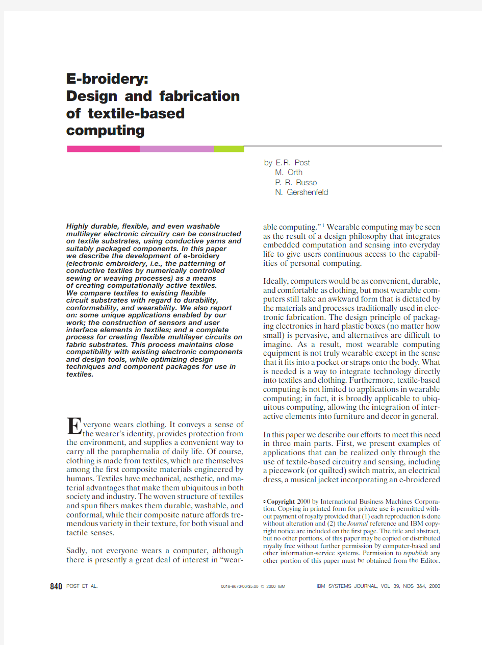
Row and column fabric keyboard.The row and col-umn fabric keyboard(Figure1)is a fabric switch ma-trix sewn from conducting and nonconducting fab-ric.The keyboard consists of two layers of highly conductive metallic organza with a resistance of ap-proximately10?/m(ohm/meter)and nonconduct-ing rows separated by an insulating layer of nylon netting(also known as tulle).When pressed at the right point,the two conducting layers make contact through spaces in the nylon netting and current?ows from a row electrode to a column https://www.360docs.net/doc/6415306138.html,-mercial gripper snaps are used to connect wires from a microcontroller to the organza.The keyboard can be repeatedly rolled up,crushed,or washed without affecting its electrical properties.
The microcontroller used to read out the keyboard was programmed to generate standard MIDI(Mu-sical Instrument Digital Interface)control informa-tion,allowing players to easily trigger different notes on an attached synthesizer.This keyboard did not mea-sure pressure information(which is important for expressive control in music).Because there was no nonlinear element present at the switching intersec-tions,false or“phantom”contacts were observed by the microcontroller when multiple keys were pressed. Finally,the piecework nature of the keyboard re-quired more manual labor than was hoped for.For all its drawbacks,however,users found it very sat-isfying to make music by crushing and crumpling this keyboard.
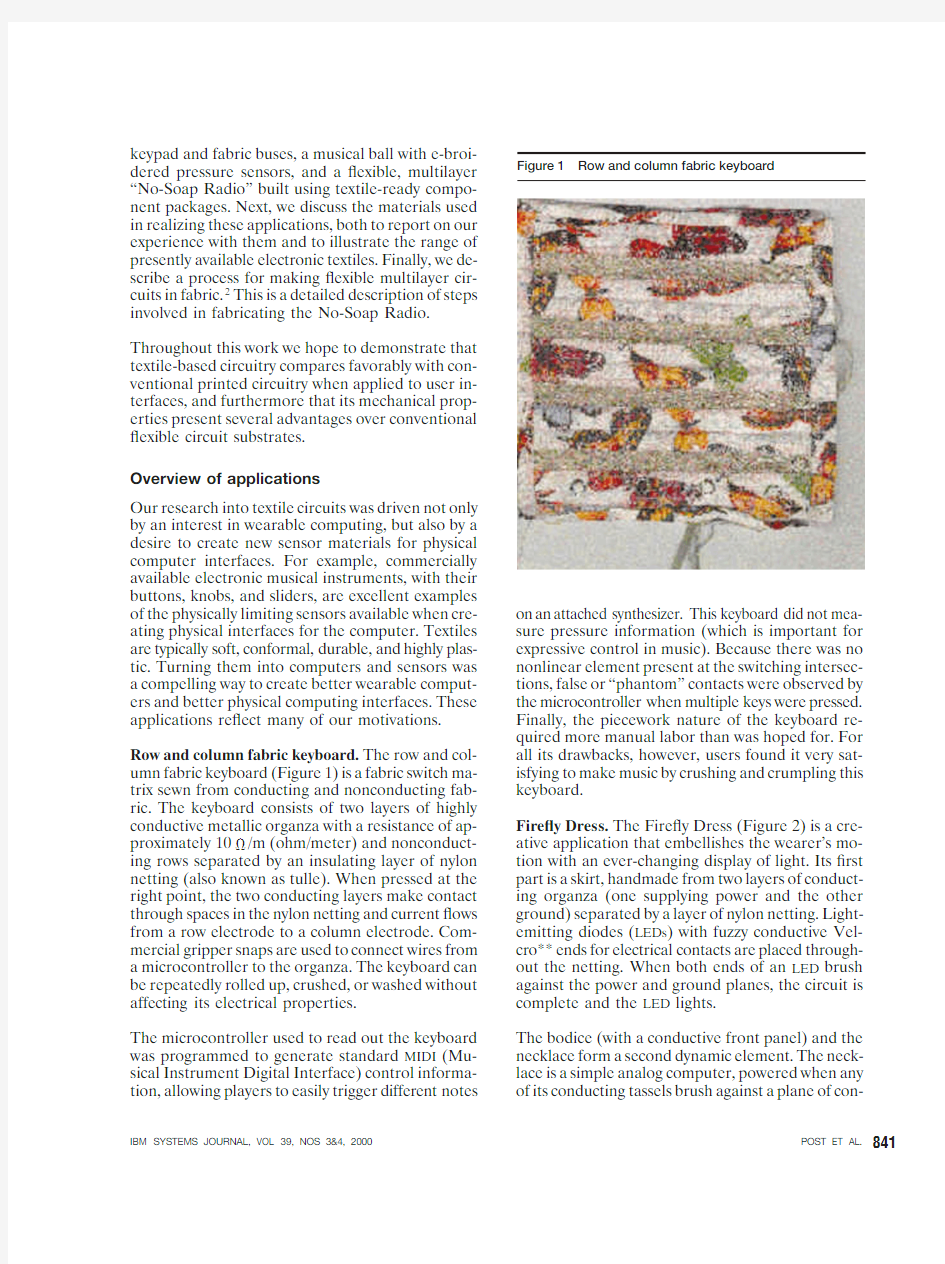
Fire?y Dress.The Fire?y Dress(Figure2)is a cre-ative application that embellishes the wearer’s mo-tion with an ever-changing display of light.Its?rst part is a skirt,handmade from two layers of conduct-ing organza(one supplying power and the other ground)separated by a layer of nylon netting.Light-emitting diodes(LEDs)with fuzzy conductive Vel-cro**ends for electrical contacts are placed through-out the netting.When both ends of an LED brush against the power and ground planes,the circuit is complete and the LED lights.
The bodice(with a conductive front panel)and the necklace form a second dynamic element.The neck-lace is a simple analog computer,powered when any of its conducting tassels brush against a plane of con-Figure1Row and column fabric
keyboard
IBM SYSTEMS JOURNAL,VOL39,NOS3&4,2000POST ET AL.841
ducting organza sewn to the front of the bodice.Each tassel has its own resistor network and provides a different color bias to the red,green,and blue LEDs on the face of the necklace.
The dress demonstrated the visual,tactile,and me-chanical potential of sewing circuitry into clothing.The dif?culty of adding ordinarily packaged LEDs to the skirt pointed out the need for more appropriate component packages.The time-consuming piece-work involved in creating the dress also motivated our search for a better means of creating textile cir-cuitry.
Musical Jacket with embroidered keypad.The Mu-sical Jacket (Figure 3)turns an ordinary denim jacket into a wearable musical instrument,allowing the wearer to play notes,chords,rhythms,and accom-paniment using any instrument available in the Gen-eral MIDI scheme.It integrates directly into the jacket an embroidered fabric keypad,a MIDI sequencer/synthesizer,amplifying speakers,a fabric bus sewn from conductive organza,and batteries to power the above subsystems.
The embroidered keypad is ?exible,durable,and highly responsive to touch.It was mass-produced us-ing ordinary embroidery techniques and a mildly con-ductive stainless steel and polyester composite thread (Bekaert BK50/2,described later),and demonstrated for the ?rst time that a textile keypad could be made by e-broidery on a single layer of fabric in one step.This process allowed us to precisely specify the cir-cuit layout and stitch pattern in a computer-aided design (CAD )environment,from which any number of articles can be sewn under machine control.The MIDI jacket keypad used a PIC **microcontroller from Microchip Technology Inc.,to perform capac-itive measurements of connections to sewn elec-trodes on a denim substrate.The measurement was implemented almost entirely in software as an ex-ercise in developing electric ?eld sensors with a min-imum of hardware,but this minimalism also bene-?ts the fabric circuit designer by reducing the number of components (and hence interconnections)re-quired in a circuit.The electrode array was sewn in the pattern of a telephone keypad,with traces lead-ing from the symbols to an array of connection pads intended to mate with a conventional circuit board.The resistivity of the electrodes and their associated connecting traces is reduced by the precise place-ment of individual stitches.Each electrode is sewn from a single continuous thread that crosses itself many times,leading to a multiplicity of intersections that create parallel resistances and increase the over-all conductivity of the sewn circuit element.By us-ing this “e-broidery stitch”we obtain resistances per unit trace length that are dramatically lower (by more than an order of magnitude)and more consistent than those obtained with conventional embroidery stitches (e.g.,satin or tatami stitches)that are cho-sen for their appearance or texture.
The embroidered keypad 3uses a capacitive sensing technique 4because of the high impedance of the sewn electrodes.The measurement algorithm is sim-ilar to that used in the Museum of Modern Art (MoMA )table described elsewhere in this issue,5but
Figure 2Firefly
Dress
POST ET AL.
IBM SYSTEMS JOURNAL,VOL 39,NOS 3&4,2000
842
here the measured capacitance is compared to a threshold to distinguish contact events.This mea-surement is implemented using a single bidirectional digital input/output(I/O)pin per electrode and a leakage resistor(which can be sewn in highly resis-tive yarn).Key contact events are output as a serial data stream by the microcontroller.The circuit board makes contact with the electrodes at the circular pads only at the bottom of the electrode pattern.A view of the component side of the circuit board has been superimposed to show its extent and its connections to the fabric.A?exible circuit board can be substi-tuted for the rigid one used in this implementation. Fifty denim jackets were embroidered with this pat-tern and out?tted with sewn fabric buses that carry power,ground,serial data and analog audio signals across the backs of the jackets.These jackets also provided an AC ground for the keypad,to ensure con-sistent capacitance measurements.In all50jackets,both the fabric keypad and bus worked reliably and held up to repeated mechanical stresses better than the more traditional wires and connectors also used. The interface between the sewn keypad and the elec-tronics led into our work to do away with the circuit board entirely.
Musical Ball.The Musical Ball(Figure4)is a plush stuffed toy that allows users to play music by apply-ing pressure in any of eight regions as they squeeze the ball.There are ten electrodes made by e-broi-dery on its surface,eight of which capacitively sense pressure and two of which provide a ground refer-ence for the capacitive sensing.The eight channels of pressure data are sent as serial data to a host run-ning an application that uses these data to generate music through either external MIDI devices or an in-ternal sound card.This application would have been impossible to realize using conventional pressure sensors.By using sensors made by e-broidery,we
Figure3On the left is the Musical Jacket,comprising a fabric keypad on one side,a MIDI synthesizer“boat”on the other side,speakers behind speaker grills in the pockets,and fabric buses visible inside the jacket.On the right is a
composite image of both sides of the circuit board attached to the back of the fabric
keypad.
IBM SYSTEMS JOURNAL,VOL39,NOS3&4,2000POST ET AL.843
were able to create a light,hand-held,?exible,mul-tichannel,continuous control instrument in a single manufacturing step.We were also able to directly tailor the sensor’s size,shape,and appearance. The impedance in the electrodes in the ball is dra-matically reduced by using highly conductive thread in the machine bobbin during e-broidery.In contrast to the electrodes in the musical jacket,whose con-ductivity is improved and controlled through stitch pattern,the conductivity of the electrodes in the ball is limited by the conductivity of the bobbin thread. Electronic Tablecloth.The Electronic Tablecloth (Figure5)is a sensor surface that allows users to in-teract with a computer and with each other in the context of a social function.Attendees identi?ed themselves to the system by setting their assigned “coaster tags”on the swirling pattern,above which are embroidered the words“Place your coaster here.”The coaster is in turn a capacitively coupled radio frequency identi?cation device(RFID)tag,and is read by the tag reader in the tablecloth when the user sets it on the swirling pattern and touches the fabric electrode on top of the coaster.The computer then enters a dialog with the user through the ap-propriate?uorescent display and keypad.
We combined?ve keypads and?ve capacitive tag readers all made by e-broidery to create a tablecloth (and centerpiece)that turns an ordinary table into interactive furniture.The electronics for this appli-cation are housed in the centerpiece.We encoun-tered dif?culty using our capacitive keys near the electrostatic tag reader electrodes,which in normal operation present a50-volt rms(root-mean-square) sine wave at125kHz to power up and read out tags. By applying a shielding layer of metallic organza un-der and around the swirling electrodes,we were able to terminate most of the electric“?eld lines”before they reached the keypad electrodes.
No-Soap Radio.This washable,crushable keypad made by e-broidery(Figure6)is known as the No-Soap Radio,because it was designed to be dry-clean-able and to transmit data to a nearby AM/FM radio (via near-?eld electrostatic coupling).When the user touches a symbol on the keypad,the microcontroller capacitively senses the contact and then transmits a particular audible tone(depending on which symbol was touched)by FM-modulating a455kHz square-wave carrier in software and presenting the resulting signal on all of the keys connected to the circuit(Pad0through Pad3).The user then acts as transmitting antenna for the No-Soap Radio.Two pins are reserved for intrasensor communications to allow the construction of larger keypads by network-ing several instances of the basic four-key sensor. Nodes can communicate with each other and a host processor over a serial bus on these two reserved pins.
The only external components used in this circuit are two2M?resistors,which allow the charging time measurement to be done in software.These are used in lieu of resistors that could be included directly in the integrated circuit.The resistors are soldered onto the PIC12C509leadframe after steel threads are mi-crospotwelded onto the leads.The resistors are in surface-mount0402packages,with dimensions0.040 inch?0.020inch?0.010inch.The fabrication of this and other,similar devices is discussed in detail below.
Textile circuit fabrication techniques
Our?rst step in manufacturing textile circuitry was to identify textiles and yarns suitable for use in fab-ric circuitry,and then to?nd a way to design and fabricate such circuitry.As piecework is time con-suming and imprecise,our primary method of cir-cuit patterning has been e-broidery,i.e.,numerically controlled embroidery using conductive thread.We use e-broidery to stitch patterns that de?ne circuit traces,component connection pads,or sensing sur-
Figure4Musical
Balls
POST ET AL.IBM SYSTEMS JOURNAL,VOL39,NOS3&4,2000 844
faces.By using commercial embroidery processes, we have built on prior art in the textile industry that permits precise control of the design,layout,and stitch pattern of the circuitry through CAD processes. Yarns and threads usable in high-speed embroidery processes must make a trade-off between electrical and mechanical properties.These yarns must be con-ductive,but also strong and?exible enough to be sewn at high speeds without breaks in either the thread itself or in the electrical continuity.These yarns must also maintain their electrical properties when washed(we consider dry cleaning to be the tar-get washing process,and exposure to water,alcohol, and sweat as an everyday occurrence).
These processes also allow control and integration of yarns with different electrical properties,for in-stance,different resistances.This level of stitch con-trol and yarn variety brings up the possibility of re-
placing discrete components such as capacitors, resistors,and inductors with speci?c combinations of thread and stitch pattern.Such components might lead to reduced manufacturing cost and higher re-liability from improved mechanical properties. Figure6The No-Soap Radio.An AM broadcast receiver (right)is used to listen to the transmitted
signal. IBM SYSTEMS JOURNAL,VOL39,NOS3&4,2000POST ET AL.845
First,in order to work with available machine sew-able threads we have chosen not to require low-im-pedance component interconnections,as is done in conventional printed circuit design.Instead,we choose circuit elements and design principles with low power consumption and high input impedances. Second,our next step was to design packages op-timized for use in fabric circuitry.In this report,we focus on the design of the“Plastic Threaded Chip Carrier”(PTCC),a package that resembles the Plas-tic Leadless Chip Carrier(PLCC).The PLCC is a well-known surface-mount integrated circuit(IC)pack-age style,designed to be soldered onto printed copper circuit traces on a rigid or semi-rigid circuit board.Conversely,the PTCC is designed to be stitched or woven into a fabric circuit,and for this purpose has long,?exible conducting leads.Our primary goal was to demonstrate a durable interconnection and attachment scheme for electronic components used in circuits made by e-broidery.
The third step was to develop multilayer circuitry. Even if we can sew a circuit,its complexity will be limited if it is restricted to lie in a plane.By making multilayer e-broidery,we hope to demonstrate that textile-based circuitry compares favorably to printed circuit boards and conventional?exible substrates in terms of design complexity and reliability,partic-ularly in user interface applications.
The?rst step in integrating electronic technology into textiles and clothing might be to simply remove the bulky and stiff housing of most electronic gear.We might also make the circuit board smaller and re-movable by redesigning it with components in smaller packages,and using conductive fasteners,like snaps, to connect the boards to the fabric.(This way the boards can be removed when a garment goes into the wash.)Unfortunately,circuit boards neither look nor feel good when they become part of clothing, nor does this approach scale well because of the many layers of packaging and connective elements that come between the silicon and the textiles.
To overcome these limitations,we have chosen to combine electronic components and conductive tex-tile circuitry as directly as possible.We replace stan-dard printed circuitry on rigid or?exible substrates with circuitry made by e-broidery and component packages optimized for use on fabric substrates. These packages can be washed without harm to ei-ther their internal electrical properties or their con-nections to the substrate and other components.Finally,we would like the interface between com-ponents and circuitry to withstand the?exing and stretching that clothing and textiles are prone to experience.
One goal of our work is to create electronic garments and textiles that exhibit integrity,that is,garments that look,feel,wash,and wear as well as ordinary clothing.In this context,system integration becomes the art of partitioning a digital system across several items of clothing.For example,most people have only a few pairs of shoes,a few more pairs of pants, several shirts,and a few outer garments.It makes sense to put the most expensive parts of a system in the shoes and outer garments,and the least expen-sive parts in the shirts,pants,and undergarments.
In this section,we discuss the properties of several textiles we have used.In the next section on com-ponent integration and packaging,we detail a strat-egy for making electronic circuitry disappear into clothing and textiles in several steps.First,we re-place standard printed circuit boards with e-broidery (embroidered textile circuitry)designed with tradi-tional CAD tools for circuit layout and rendered on numerically controlled embroidery machines using conducting and insulating threads.Second,we re-design electronic component packaging for use in circuitry made by e-broidery.Third,we combine lay-ers of circuitry to form multilayer circuitry of arbi-trary complexity.
Existing?exible circuit substrates.Many methods already exist to fabricate circuits on?exible sub-strates.Most of these rely on the metallization of a ?exible polymer substrate that can withstand the high temperatures of conventional soldering processes. Kapton**(polyimide)?lm,for example,is one of the most commonly used?exible substrates,typically ?nding applications in cameras(where circuitry must ?t intimately into available space in a small pack-age),printers and portable computers(where a num-ber of connections must cross a hinge or other ro-tating joint),and nonplanar antennas(where the antenna elements must have accurate dimensions yet be shaped to?t on conical forms).
When circuitry is designed for such a substrate,care must be taken to ensure that in the?nal application mechanical stress will not be applied to the compo-nent-circuit solder joints.Because of this,the param-eters of motion of the?exible substrate must be well understood at the time of design.That is,the mo-tion of conventional?exible substrates must be con-
POST ET AL.IBM SYSTEMS JOURNAL,VOL39,NOS3&4,2000 846
strained to ensure that they continue to work over their expected lifetime.In general,conventional?ex-ible substrates are?exible only in regions where com-ponents are not attached.
Our dissatisfaction with conventional?exible sub-strates stems from the fact that they cannot be crum-pled nondestructively in the way that cloth can be. To be clear,by“crumpling”we mean simultaneously folding the substrate along multiple nonparallel axes.
Flexible multichip modules.An interesting excep-tion to our ruling against conventional?exible cir-cuitry might be the?exible multichip module(MCM), an example of which is shown in Figure7.This mod-ule is the result of collaboration with workers at the Charles Stark Draper Laboratory at MIT to produce small,semi-?exible circuit elements that may be em-bedded in textile products to form a sensor readout network.We make an exception in this case because of the module’s small size.
The major part of this readout element is a PIC16F84 microcontroller IC,visible underneath the titanium-copper interconnections.In addition to the PIC16F84 there are four3M?chip resistors and a16pF(pi-cofarad)chip capacitor.The schematic for the MCM is similar to the circuit used in the fabric keypad in its simplicity and choice of microcontroller.In this case,the host attaches to the RB7and RB6pins, which form a full-duplex(RS232)serial data link op-erating at9600baud.The connections are formed by drilling out the centers of the pads and inserting a small pin or rivet to pressure-?t each pad to a mat-ing circuit trace made by e-broidery.Power for the circuit is supplied across the V dd and V mm pins,and electrodes are connected to the Trode[0–3]pins to be capacitively read out just as was done in the orig-inal fabric keypad.
The entire?exible MCM measures0.600inch?0.300 inch,is0.016inch thick,and has a permissible bend-ing radius of curvature of about50centimeters(cm). In a fabrication process similar to that developed by the General Electric MCM-E/F group,6the constit-uent components were thinned to0.006inch by me-chanical grinding and lapping of the rear face of each component.The components were then placed on a rigid substrate,a laser-cut0.006-inch Kapton mask was applied to planarize the top surface,and the Ti/Cu(titanium/copper)interconnect was deposited through a stencil mask.This process extends readily to multilayer circuitry by the addition of thin(0.001-inch)insulating layers.Finally,a protective Kapton cover was glued to the top of the circuit module.The module was then removed from the rigid substrate, and a Kapton cover glued to its bottom,resulting in a completely encapsulated element.
Previous work in conductive textiles.The state of the art in textile circuitry seems to be largely unpub-lished and proprietary.While a great deal of work has been done in the?eld of electrically active tex-tiles,we have not been able to?nd(at the time of this writing)any published prior art relating to ei-ther the layout and sewing of active circuitry on tex-tiles with conductive yarns,or to the integration and attachment of off-the-shelf or specially designed elec-tronic components onto textile circuitry.However, there is related work which could enable the devel-opment of conductive textiles with active circuitry.
A survey of the U.S.patent literature reveals much ongoing work focusing on the development of syn-thetic conductors compatible with existing textile production processes.For example,7,8there are con-ductive polymers that remain fairly conductive(?1?/cm)after being spun into threads having the weight,strength,and appearance of ordinary nylon thread.
In other potentially enabling developments,for ex-ample,workers at Motorola have patented IC pack-ages with hook-and-loop fasteners9as a means of attaching components to conventional?exible sub-strates.10Such packages—if successful—might do away with the complex art of surface-mount
solder-
IBM SYSTEMS JOURNAL,VOL39,NOS3&4,2000POST ET AL.847
ing and its associated environmental burdens.In an-other patent,workers at IBM proposed a zippered connector to simplify the assembly of wide backplane interconnections.11
Other researchers are embedding photonic conduc-tors(optical?bers)into clothing to build architec-tures for sensing and data distribution.The sensate liner12is one such undergarment,in which a woven ?ber optic matrix is used to sense disruptions of the weave(by measuring optical continuity)and to per-form spectrographic analysis of the materials present at intrusions.Such analysis can be used to determine the type and severity of wounds suffered by the wearer of the liner.While this work is promising be-cause of the variety of?ber optic sensors that can be made,drawbacks arise at the interfaces of the op-tical?bers to the conventional electronics that are required for signal origination and processing.
Conductive yarns,?bers,and textile substrates.The textile circuitry in this paper includes sewn or stitched textile circuit elements that function as conductive traces,sensor elements,electrodes,and discrete com-ponents(e.g.,resistors and capacitors).Many tex-tiles and yarns have properties that suggest their use in such fashion.There are also a number of man-ufacturing processes that could produce these fab-ric circuit elements.
An ideal yarn or textile for fabric circuits would have completely adjustable electrical properties and would maintain those properties while being sewn,?exed, and worn.In this section,we identify and describe the strengths and limitations of some of the mate-rials that have been useful in our work.In outlining our practical knowledge of a variety of materials and processes for creating fabric circuits,we can at best hope to inspire the creation of new textile forms op-timized for use in circuitry.
Metallic silk organza.In its primary form,this is a ?nely woven silk fabric with a thin gold helix wrapped around each thread that runs along the weft of the weave(Figure8).Believed to have originated in In-dia,this sort of fabric has been produced for cen-turies and appeared in Western fashion as early as the mid-18th century.13The warp of this fabric con-sists of parallel silk threads.Through this warp,the weft is woven with a silk thread that has been wrapped in a metal foil helix.This metallic thread is prepared just like cloth-core telephone wire,and is highly conductive(?0.1?/cm).Because the con-ductors in this fabric only run in one direction,the fabric is anisotropically conductive.The spacing be-tween these?bers also permits them to be individ-ually addressed,so a strip of this fabric can function like a ribbon cable.If a section of organza is sub-jected to shear,the cells formed by the weave also shear to form parallelograms,keeping the conduc-tive?bers parallel and separated at all times.The silk?ber core has a high tensile strength and can withstand high temperatures.
Circuits fabricated with components attached to or-ganza only need to be protected from folding con-tact with themselves,which can be accomplished by coating,supporting,or backing the fabric with an in-sulating layer which can also be cloth.However,ev-idence shows that coating can disturb the conduc-tivity of the fabric.Circuits formed in this fashion also have many degrees of?exibility(i.e.,they can be wadded up),as compared to the single degree of ?exibility that conventional substrates can provide. In the microcontroller circuit shown in Figure9,a PIC16C84microcontroller and its supporting compo-nents are soldered directly onto a patch of metallic organza.This circuit uses bidirectional I/O pins on the PIC to control LEDs and to sense touch along the length of the fabric,and uses audible feedback through a piezoelectric speaker to reinforce the sense of interaction.All of the components are soldered directly onto the surface of the metallic organza weave except for the microcontroller,which sits in a socket soldered to the organza.
Figure8Micrograph of woven metallic organza.The two
horizontal threads are wrapped with a metal
foil.
POST ET AL.IBM SYSTEMS JOURNAL,VOL39,NOS3&4,2000 848
While the copper,gold,or silver foil wrap the silk thread,the foil’s fragility makes it impossible to ma-chine sew without damaging the wrap and breaking the electrical continuity.Consequently,this mate-rial was used to create labor-intensive piecework cir-cuits,or as the substrate for component attachment. In piecework,many drawbacks of the material ap-peared.Because the material is anisotropically con-ductive,it was necessary to tie the conductors to-gether either with a perpendicular conductive band or by folding the material over itself.All this was time consuming and labor-intensive.Finally,the standard copper and silver coatings on the material will cor-rode over time unless they are properly passivated. Conductive yarns.The conductive stainless steel yarns outlined in this subsection were initially manufac-tured to make?lters used in processing?ne pow-ders.Stainless steel presents some immediate advan-tages.It is inert and therefore not sensitive to washing or sweat.These stainless steel yarns vary in compo-sition,from100percent continuous conductive steel ?bers to feltings or composites of polyester and with short steel?bers interspersed throughout.Varying the ratio of the two constituent?bers leads to dif-ferences in resistivity.The conductivity of these yarns is also ultimately limited to the conductivity of the stainless steel?bers themselves.Their conductivity is limited by their manufacturing process,by cold working,and their?ne diameter,which makes them sewable.
Bekaert Fibre Technologies14credits a1936U.S. Patent15with the original description of the process whereby a bundle of?ne metal?bers may be drawn continuously and simultaneously from source met-als.Bundle-drawn?bers can be produced in many different morphologies by translating the polymer-based methods of the synthetic textile industry into their metallurgical equivalents.Continuous and bro-ken bundles,cut?bers,spun yarns,threads,etc.,are all produced in this way.
The?bers themselves are available in diameters from 100?m(micron)to12?m,and as small as2?m for very metallurgically clean(free of large inclusions) alloys.Alloys commonly used in these processes in-clude stainless316L steel,stainless302steel, Inconel**601,NiCr(nickel-chromium)and FeCr (iron-chromium)alloys,and titanium.14These100 percent metal?ber yarns are used in knitting,weav-ing,needlepunching,and braiding processes,with sewing and embroidery being notable omissions from the list.
Figure9Circuit fabricated on metallic
organza
IBM SYSTEMS JOURNAL,VOL39,NOS3&4,2000POST ET AL.849
Bekaert Fibre Technologies 14cites the primary ap-plications for these materials as being ?lter media,antistatic textiles,heat-resistant textiles,burners,and conductive plastics.Their product range includes 100percent metal ?ber products as well as blends of metal ?bers combined with natural or human-made ?bers.Steel threads were chosen for their strength,resistance to corrosion,biological inertness,and ready availability in textile form at low cost.The ma-jor drawback of using steel and steel-composite threads is the dif?culty involved in attaching them to existing electronic components.
Composite yarns of short steel ?bers and polyester were chosen for machine embroidery because an all-steel continuous ?ber thread (used to form compo-nent leads),cannot be sewn by machine.In a con-tinuously drawn steel ?ber bundle,individual ?bers are meters (rather than centimeters)long.Stresses are no longer local to a small region of sewing,and tensions rapidly mount without resolution,resulting in bunching of the thread as it feeds through the sew-ing machine.Some of the bunched threads will even-tually twist into an obstruction that will not pass through the sewing needle’s eye,and the entire pro-cess will grind to a halt.In contrast,threads spun from short (staple)?bers are able to accommodate this variation in tension by stretching.Following is a list of ?bers we have studied:
●
BK 50/2(?50?/cm)—This composite thread,while being highly resistive,performs the best un-der machine sewing and passes through ordinary sewing needles better than any other conductive thread we have used.Both the magnitude and con-sistency of this thread’s conductivity can be con-trolled by careful stitch placement,which deter-mines the intrathread conductivity as a function of thread crossings as well as interthread conduc-tivity as a function of thread https://www.360docs.net/doc/6415306138.html,e of this thread in both the needle and the bobbin dramat-ically increases the conductivity of stitched traces.The thread comprises a spun felt of short (?1-inch)steel and polyester ?bers (see Figure 10).Because the steel ?bers are short and extend from the body of the thread,short circuits can occur be-tween sewn traces.This can be corrected after the traces have been sewn by brushing the fabric with a sponge-covered magnet.These same extending steel ?bers provide an excellent contact surface.This is important for pads that make contact with circuit boards (as in the Musical Jacket),pads meant to contact skin for sensing,and contact be-tween separate threads and traces (particularly in the case of vias in multilayer circuitry made by e-broidery).
●
Bekintex 100percent stainless steel continuous ?-bers (?1?/cm)—These threads comprise bundles of continuous cold drawn stainless steel ?bers (see Figure 11).The ?bre is highly conductive,but can-not be machine sewn because of its low elasticity.The single-ply version of this thread will not hold
Figure 10
Photomicrograph of BK 50/2.The dark,unruly fibers are stainless steel,in a polyester
mesh.
Figure 11
Photomicrograph of Bekintex single-ply
continuous-drawn stainless steel fiber
bundle
POST ET AL.
IBM SYSTEMS JOURNAL,VOL 39,NOS 3&4,2000
850
a knot,but the two-ply version(BK12/2?275/175S)will,because the plies are tightly twisted. These threads are suitable for microspotwelding to component leadframes and are used to repack-age components with threaded connections.Al-though they are unsewable,these threads can be couched(attached to a substrate by a covering stitch);this is the technique used to attach com-ponent leads to e-broidered circuits.
●Bekintex15/2100percent stainless steel spun?-bers(?1?/cm)—An alternative to the continu-ously drawn steel?ber bundle is an all-steel yarn spun from short steel?bers.This thread is ma-chine-sewable and performs well in the bobbin of commercial embroidery machines.Its main draw-backs are due to its“untidiness”;although it con-tains a far larger number of short stainless steel ?bers than its BK50/2counterpart,these?bers are not held in place by a polyester mesh.As a result, many more steel?bers free themselves from the thread body,causing short circuits between traces and irritation of the wearer’s skin.
●VN140nyl/35?3(?10?/cm)—This thread is
a nylon core wrapped with three continuous cross-ing stainless steel?bers.It is relatively sewable through needles and highly sewable in the bobbin of commercial embroidery machines.Electrodes sewn with this thread are limited by the conduc-tivity of the steel?bers.Because it has no loose ?bers,it creates fewer short circuits between traces. Electrodes sewn with this thread are highly dura-ble and conductive.Because it has no loose?bers, it also presents less electrical contact area,mak-ing electrical connection dif?cult.
●Aracon**metal clad aramid?bers(MCAF)yarns (?0.001ohm/cm)—Recently the DuPont company announced their Aracon MCAF yarns.16These yarns comprise anywhere from24to200conduct-ing?bers,each approximately15?m wide.The aramid core of these?bers is usually Kevlar**, while the cladding metal is silver(Ag),nickel(Ni), copper(Cu),gold(Au),or tin(Sn).Ag and Ni clad-ding are preferred for the aerospace applications that DuPont has targeted as their initial market, where the bene?t of a40–60percent mass reduc-tion outweighs the added cost of what is presently a very expensive composite?ber.
Aracon exhibits excellent mechanical and electri-cal stability over repeated?exures,radiation ex-posure,and changes in temperature.Because the
aramid core can withstand high temperatures and has a thermal coef?cient of expansion similar to that of the cladding metals,Aracon can be sol-dered like normal wire.Because of these prop-erties,as Aracon comes to be mass-produced and its availability increases,it is likely to emerge as a material of choice for unexposed fabric circuitry. Composites made by e-broidery.One technique we are developing is the stitching of composite traces. Suppose that a Bekintex15/2stitch is covered by a BK50/2overstitch.Segments of the trace that cover the steel bundle will exhibit much lower resistance per unit length than segments of BK50/2alone.As discussed above,the conductivity of the all-steel yarn is about100times greater than that of the compos-ite yarn,which implies that low-precision resistor net-works can be constructed simply by combining runs of stitches in the two materials.It also leads to the more general notion of a composite trace or sensor comprising materials combined by stitching. This technique can also be used to build coaxial struc-tures.One particularly useful example is that of cov-ering a conductive trace with an insulating stitch to protect the former from coming into accidental con-tact with other conductors.
Component integration and package design in textile circuitry
As a consequence of the design principles mentioned above(i.e.,distributed sensing and computation,thin interconnect,small packages with fully integrated cir-cuitry),components destined for placement in fab-ric circuitry do not demand high connection densi-ties.Most component packages are optimized for joining to printed circuit boards,so we instead op-timize them to interface with textile circuitry.Ulti-mately,we hope this work will lead to an actual pack-aging standard used by the integrated circuit industry.
Fabrication techniques.There are several ways to embed electronic circuitry in fabric,depending on the choice of substrate.Some possibilities explored in the course of this work include:
●Soldering surface-mount components directly onto metallic organza
●Bonding components to a substrate using conduc-tive adhesives
●Stapling components into a conductive stitched cir-cuit(i.e.,pressure-forming their leads to grip cir-cuit pads)
IBM SYSTEMS JOURNAL,VOL39,NOS3&4,2000POST ET AL.851
●Joining a component’s“threadframe”directly to
a stitched fabric circuit(where components are formed with a single conductive thread per pin) The last possibility is explored in some detail in the following section.We have ruled out the others for various reasons indicated below:
●Solders used with electronic components are soft alloys of lead(Pb),tin(Sn),and sometimes silver (Ag).Such compounds are not suitable for use in applications in which they could potentially be in constant contact with a user’s body,because of their toxicity.Worse yet,while it is possible to sol-der components onto metallic organza and achieve (very)good electrical contact,the mechanical properties of the joint are unsuited to the?exure to which it will be subjected as an item of apparel.
●Conductive adhesives are better suited to this ap-plication than solder,because it is possible to en-vision adhesives that are nontoxic,highly conduc-tive,highly durable,and moderately?exible to act as a“mechanical impedance match”between a ?exible fabric substrate and a rigidly packaged component.They remain an open possibility and should be the subject of further study.
●Stapled components are an interesting compro-
mise where a component lead grips a sewn con-ductive trace by being pressed into shape around it.When the substrate?exes,the trace is free to move within the clasp of the formed lead,forming a self-wiping contact at every junction between fab-ric circuitry and component pins.However,the di-mensional rigidity of the component is a poor match for freedom of motion enjoyed by a fabric substrate,and the mismatch is likely to stretch open pins that have been formed into clasps and to ac-celerate wear and tear of the fabric substrate. Gripper snaps make excellent connectors between fabric and electronics.When a two-piece gripper snap is placed on fabric,the?rst piece has several metallic“teeth”that pierce the substrate and any conductors,making a wiping contact that scrapes through surface contaminants(e.g.,oxides)to make a metal-on-metal bond.They are already commonly used to connect circuit packages to fabric,but allow only a low connection density.
The case for round packages.Consider electronic components with threads leading out from the pack-age rather than a rigid leadframe.These threads may be attached to the substrate by covering stitches that also form electrical connections to circuitry made by
Figure12Square and radial PTCC packages
STEEL/NOMEX COMPOSITE THREADS
POST ET AL.IBM SYSTEMS JOURNAL,VOL39,NOS3&4,2000 852
e-broidery.Alternatively,the threads emanating from a component may be punched or woven through the substrate on their way to connect to other components.In either case,these threads con-strain the components to their location on the sub-strate.Because we would like to balance as evenly as possible the forces conveyed by these threads,we now consider round component packages.Figure 12illustrates components in square and round packages stitched onto a fabric substrate,whereas Figure 13shows an actual stitched prototype component couched onto a fabric substrate.
For a given lead spacing (s )at the periphery of a package and a given package diameter (d )or side length (l )the maximum number of threads coming out of each type of package is found to be n square ?4
?l s
?1?
n round ?
?d
s
For a given thread spacing around the periphery of the package,it is clear that for a large number of pins the square package will have a smaller diam-eter than the round package.If the number of pins is less than 16(or to be exact,16(4??)?4),then the round package makes better use of the available space.
The ?nest practical thread spacing achieved in our work has been 0.050inch (1.27millimeter),which for 16leads implies a package diameter of 0.254inch (6.48millimeter).It is practical to expect that a die of about half this width will ?t into the package,which gives an upper bound of 10mm 2of single-or multi-chip real estate to work with in a typical sewable but-ton package.
The plastic threaded chip carrier.Now we look to the practical aspects of building packages like those that have been described so far.To manufacture threaded packages,we would start with a bare die,add a “threadframe,”and connect the near ends of the threadframe to the bondout pads of the die.Figure 14shows the possible construction of such a component package.Some details have been omit-ted for clarity,such as the metal base that helps to keep the die substrate at near-uniform temperature and electrical potential across its area.
Connections directly to the die are made in the usual way;?ne gold wires are thermocompression-bonded on one side to the die’s gold-plated “bondout pads”and on the other to the stubs of a conventional cop-per leadframe.
Figure 13
Prototype PTCC package couched onto fabric
substrate
Figure 14Details of round PTCC construction
INTEGRATED IBM SYSTEMS JOURNAL,VOL 39,NOS 3&4,2000
POST ET AL.
853
In most packages,the leadframe continues out of the plastic package and is ultimately soldered or cold-welded to external circuitry.Instead of having a solid external leadframe,the plastic threaded chip carrier (PTCC)has?exible,corrosion-resistant threads in-tended to connect to external circuitry.
In this case,the threads that leave the package are bundles of approximately100continuous steel?bers, each about5?m in diameter.These?ber bundles are microspotwelded to the leadframe stubs,and the entire structure is hermetically sealed in a plastic car-rier.
Prototyping the PTCC.To test the proposition of a threaded chip carrier,prototypes were built to eval-uate their electrical,mechanical,and sartorial per-formance.
Since part of the PTCC’s assembly process is common to most IC packages,we can test the design princi-ples behind the PTCC without building one com-pletely from scratch.Leaded surface mount(SMT) IC packages already incorporate the die,the lead-frame,and bonding wires in a sealed plastic carrier, and their electrical characteristics are well under-stood.
Prototypes have been built by starting with SMT pack-ages,adding a few components directly to the leads, then microspotwelding steel?ber bundles to the leads.Finally,the threads are arranged in a radial pattern,and the entire assembly is encapsulated in an epoxy resin.
Packages made this way are larger than they need to be,but all of the new design principles involved are represented and open to re?nement.
Spot welding.Elihu Thompson pioneered electrical or resistance welding in the late19th century,17tak-ing advantage of the fact that an electrical current passing through any resistive material evolves heat.
For constant-current welding the heat evolved per unit area?Q takes the form
?Q?I w2R
A?t
where I w is the weld current,R is the weld junction resistance,A is the weld junction area,and?t is the weld time.The welding apparatus is arranged so that most of the weld power is dissipated at the faying interface, which is the junction of the materials to be welded. Inspection of the heat evolution equation reveals that for a given weld current and time,the weld heat in-creases directly in proportion to the junction resis-tance and inversely in proportion to the junction area.This suggests that the resistivity of the weld path should be concentrated at the weld junction,and that the junction area should be small.Resistive heating is only part of the story,however.Although a large area of contact is desirable between the electrodes and the workpiece to reduce heating at those points, a small electrode-workpiece junction area is pre-ferred to reduce heat diffusion from the faying in-terface.When two uniform,smooth pieces are welded together,the heating will be greatest along the center axis of the applied current,and a weld will form between the pieces along this axis.The heating is greatest along the center of this axis,be-cause at that point the weld is most surrounded by heated material.Different types of welds will arise from different levels of heating.The“coldest”welds form when the grain boundaries of the workpieces shift to form large interfaces.As heating increases, grain boundaries shift and dovetail,forming a com-plex interface.Still greater heating results in a break-down of grain boundaries and a variable alloying of the materials making up the junction.The leadframe used in this case was copper(Cu)plated with a tin-lead(SnPb)alloy.Diffusion alloying takes place at the Cu-SnPb interface,and the result after several hours is a Cu-CuSn-SnPb interface.This chemistry is common to the process of soldering with SnPb al-loys on Cu or CuSn surfaces.
It is worth noting that while the process described here was developed using Cu plated with SnPb,our goal is to produce component packages that expose only biocompatible materials(e.g.,the stainless steel threads).Furthermore,the process is compatible with uncoated Cu leads,making SnPb altogether un-necessary.
Bondout metallurgy.Weld schedules are often dif-?cult to optimize,and depend crucially on many fac-tors including electrode geometry,contact area,and electrode-workpiece metallurgy.For instance,we might wish to attach steel threads directly to the bondout pads of an IC die without using an inter-mediate Cu/CuSnPb leadframe.This is impractical for many reasons.
POST ET AL.IBM SYSTEMS JOURNAL,VOL39,NOS3&4,2000 854
Steel threads are too strong to be thermocompres-sion bonded to metallized pads on a crystalline sil-icon substrate without causing the substrate to crack.18More important,however,is the metallurgy of bondout pads on silicon chips.
Most ICs use Al(aluminum)metallization for on-chip interconnections,as well as for bondout pads. Nearly all pad-to-leadframe wirebonds take place us-ing Au(gold)or Al wire(actually99percent Al?1percent Si).Au is used more frequently because it requires less preforming during the wirebonding procedure and because it forms less of a surface ox-ide layer than Al wire does.Bondout pads are also usually plated with Au(over the Al)to promote good wire-to-pad bonding.
The Au-Al interface does,however,represent a com-promise between the need to achieve a strong wire-bond and the need to develop a process insensitive to contamination.The most common reliability prob-lem in wirebonding results from the formation of in-termetallic compounds at the Au-Al interface,known by their color as“purple plague”(AuAl2)or“white plague”(Au5Al2).These compounds are very brit-tle compared to the metallic Au and Al that surround them.Because of this brittleness,wire?exing(as a result of vibration or thermal cycling)more easily induces metal fatigue and stress cracks.18These and other intermetallic compounds and alloys deleteri-ous to the strength of the Au-Al interface are known to form more readily in the presence of all of the metals that Bekaert produces in textile form.It is therefore essential to ensure the purity of the gold used in plating bondout pads,as well as the purity of gold wire used to bond to the gold-plated pad. For the present work,weld schedules have been de-veloped to maximize the pull strength of the thread-leadframe junction.To prevent interference that would be caused by fraying of the end of the?ber bundle,it is?rst welded by one or two weld oper-ations.The tab is then cut in the middle and the ex-cess length is discarded.To weld this tab to the lead-frame,the tinned copper leadframe(Cu/SnPb)is placed on the lower electrode,the steel?ber bundle tab is placed on top of the lead,and the upper Cu electrode is brought down to weld the tab to the lead at an applied force of16pounds.
Other weld schedules,geometries,and electrode ma-terials have been tried with varying degrees of suc-cess.To minimize the number of tool changes nec-essary during weld process development,an
Figure15Two views of microspotwelding
rig
IBM SYSTEMS JOURNAL,VOL39,NOS3&4,2000POST ET AL.855
electrode geometry has been chosen to simulta-neously provide a good mix of thermal,electrical,and mechanical properties,and is shown in Figure 15.
The upper electrode is formed from 1
8-inch diam-eter copper rod stock,with the end ground down to
a 18-inch ?1
16-inch rectangular cross section.The lower electrode is formed of 18-inch copper rod with
a 1-inch ?34-inch ?1
16-inch copper “anvil”soldered on top.The anvil provides a thermal sink that draws excess heat away from the weld,decreasing the ten-dency of the electrodes to stick to the weld and pro-moting even heating (and therefore,uniformity)of the weld joint.A representative weld joint of a stain-less steel thread to Cu/CuSnPb lead is shown in Fig-ure 16.
Weld evaluation.The mean shear strength of a weld formed by the above procedure is 36.8N (standard de-viation ?4.3N,n ?9),determined by pull testing.Welds with a pull strength less than 10N were discarded (3out of 12samples tested)as being the result of poor process control or weld contamination.During these tests,most failures occurred at the point where the leadframe entered the plastic package,not at the thread-leadframe weld itself.That is,the weld joint proved to be stronger than the leadframe itself.A pull strength of 36.8N (or equivalently,8.25pounds)is more than suf?cient for the application described above,e.g.,that of welding steel threads to leadframe stubs prior to encapsulation in a her-metically sealed plastic package.It also suf?ces for the purpose of prototyping such packages,where steel yarn is welded to the leads of an existing pack-age and the resulting construction is encapsulated in epoxy.In both of these applications,the pull strength of the original weld is augmented by the ad-hesion of the thread to the package encapsulant.Multilayer textile circuitry.The leap from single lay-ers of e-broidery to multilayer circuitry is motivated not only by the desire to develop nontrivial inter-connects and circuitry,but also by the need to con-trol the outward appearance of fabric interfaces.Fab-ric-based user interfaces should at large display only devices and symbols relevant to user interaction,and not the underlying complexity of their implementa-tion.In adopting the modular approach to circuit fabrication,we have so far developed circuit design techniques,component packages,and a method of “printing”an interconnect in fabric.All of this leads to the ?nal step of stacking fabric layers with an in-sulating layer and adding an interlayer stitched in-terconnect.The way this is done with conventional circuit boards is to print each layer in copper on one side of a thin substrate,then to laminate the strata together,drilling holes as is appropriate,and to plate with copper to interconnect traces on different strata.The interlayer connections are commonly referred to as vias,and the metallurgy and chemistry of this process is messy and expensive.
To do the same thing in fabric,however,we have an easier time.Each layer of the interconnect is made by e-broidery on its own fabric substrate.Then in-sulating fabric layers are placed between the layers with circuitry,and vias are stitched between layers using more conductive thread.
Suppose we want to build an interface that has only buttons on its top surface,such as the No-Soap Ra-dio.How can this be done?
First,we make a plane by e-broidery with nothing but the interface objects sewn in.The next layer is simply a thin,sturdy insulating layer,followed by an-other layer with circuitry.This second layer of cir-cuitry includes pads that line up with the interface symbols on the top layer.The next layer is again an insulator,and the last layer includes the components that have had their leads couched onto the fabric substrate connecting to traces,some of which include pads to connect with other layers.Finally,the layers are assembled and stitched together at points where signals must cross between layers.
To enhance the ?nal appearance,the topmost layer is the last one to be quilted onto the remainder.This avoids sewing vias through the top layer for any con-Figure 16
Top view of a stainless steel thread welded to Cu/CuSnPb
lead
POST ET AL.
IBM SYSTEMS JOURNAL,VOL 39,NOS 3&4,2000
856
nections other than those required by the top layer. The principle is illustrated in Figure17.
Capacitive contact and proximity sensing.Brie?y, the increase in a sewn electrode’s capacitance due to?nger contact is measured in terms of the time taken to charge the electrode/?nger capacitance from zero to the switching threshold voltage of a CMOS (complementary metal-oxide semiconductor)logic buffer(1/2Vcc or supply voltage).
One form of the instrumentation for this measure-ment is illustrated in Figure18.The main advantages of this technique are that it is a time-domain mea-surement,it provides a dynamic range of104,and it can be implemented with little more than standard CMOS logic.Not only can direct contact be measured,
but the dynamic range also permits noncontact sens-ing to occur over a distance roughly twice as far away from an electrode as the electrode is wide.
There are also a number of ways to re?ne the dy-namic range of the measurement in software.For example,the measurement granularity of the charg-ing interval is ultimately limited by the length of the software loop which performs the time count.Nor-mally one might discharge the capacitors,then turn on the charging signal and count the number of it-
Figure17Exploded view of No-Soap Radio showing stitched vias
TOP ELECTRODE
INSULATING
BOTTOM CIRCUIT
Figure18Schematic of No-Soap Radio
IBM SYSTEMS JOURNAL,VOL39,NOS3&4,2000POST ET AL.857
erations of a fast loop that elapse before the capac-itor voltage exceeds the input high threshold. Instead of letting the capacitor charge continuously, however,the software timing the charging curve can transfer small pulses of current on each iteration, meaning that each tick of the counter corresponds to a smaller portion of the charging curve.
For the MIDI jacket keypad,such careful measure-ments were not used.Instead,a simpler procedure was employed,with each electrode permanently con-nected to analog ground through a1-M?resistor, to allow the measurement of the discharge curve of an electrode.For later systems,however(including the?exible MCM and the washable keypad),the tech-nique described above was employed.
Future work
What remains to be done?The present work col-lects our observations and experience over three years of work with fabric circuitry in a desire to point the way toward scalable processes for the manufac-ture of washable computing systems.It is expected that the primary uses of such systems will be as in-terfaces to more commonplace devices,such as pag-ers,phones,and wearable computers. Regarding washability,e-broidery will not currently function when wet,but works?ne when dried again. Whether the wetting agent is water,isopropyl or ethyl alcohol,or one of the common dry-cleaning?uids, once the circuit is dry it functions as speci?ed.Al-though rigorous testing remains to be done,the early indications are very promising.Even human sweat (a mildly corrosive saline condensate)does not ap-pear to harm e-broidery over several cycles of ex-posure,while it does in fact corrode conventional tinned-copper printed circuitry.
The threadframe prototypes have been surprisingly robust,and further work should be done to charac-terize their integrity over many stress cycles.Since the stainless threads used in this work are composed of many long,thin?bers,we would like to know how likely an individual?ber is to break when the entire thread containing it is subjected to stress.
What if you want to change your clothes?This is an open research question that might best be addressed by ongoing efforts into building environments that support mobile agents in embedded applications. One vision of the washable computer of the near fu-ture is a jacket with many small computing elements distributed throughout,all interconnected by a stitched network.Each node would provide sensing in its physical locale,some storage for a distributed, redundant database,and a computing element ca-pable of executing small mobile applications.A jacket or vest could easily host a hundred such small nodes(an added weight of about50grams or2ounc-es),and be powered all day by a battery slipped into a pocket.When you hang up your jacket,it joins the closet network and synchronizes itself with other ar-ticles of clothing and the network at large.The sce-nario is easy to construct given an embeddable sub-strate for mobile code.
Clothing is also interesting because it can augment intrabody signaling19and power transduction20tech-niques.The capacitive links to the human body that these depend on are limited by the total area of ca-pacitive contact available at each link.By transmit-ting power harvested in the shoes through the body to a large receiving electrode in the jacket,ef?cien-cies should be realized that are suf?cient to replace the need for batteries.
Much work remains to be done in replacing Beki-nox and Bekintex with other composite textiles de-signed to withstand corrosion,to allow easy welding and sewing,and to have higher conductivity.We also foresee a way to replace batteries,by collecting the triboelectric currents that cause charge migration and “static cling,”but this will require careful attention to the topology and chemistry of weaves intended to generate power.
Many interesting proposals to make wearable infor-mation infrastructures suggest the application of highly redundant optical?ber networks in clothing. We do not see e-broidery as a replacement for op-tical?bers,but rather as a complement.E-broidery excels at certain things when compared to optical ?ber,but?ber also has its?ne points.Many success-ful systems are likely to stem from a clever combi-nation of the two.
Apart from e-broidery,electrospinning21may also be a viable way to place electronic textiles on a substrate. It may turn out to be a good way to bond compo-nents to circuitry made by e-broidery,for example, by allowing one to deposit polymer meshes of dif-ferent properties onto an existing cloth substrate.In electrospinning,the force of electrostatic repulsion is used to generate a?ne,splaying jet of polymer (from a droplet of melt or solution)that forms a mesh
POST ET AL.IBM SYSTEMS JOURNAL,VOL39,NOS3&4,2000 858
at an electrically grounded collection surface.This may be better than spot-welding or applying conduc-tive adhesives because electrospinning is guided by electric?elds,so the spinning process will presum-ably extend previously deposited conducting paths and ensure their continuity.
Electrospinning is compatible with the needs of washable computing because it deposits a permeable mesh,rather than a solid,impermeable layer(as would silk-screening or printing).Materials spun into mesh form can have a better strength-to-weight ra-tio than in the solid form,as well as greater?exi-bility and breathability.By electrospinning with con-ductors,semiconductors,and insulators,one might effectively print and encapsulate multilayer electronic structures.Wearable displays could also be formed by combining electronic ink with an electronic tex-tile substrate.22Large sensor surfaces are worth ex-ploring.Textiles range in scale from small pieces of needlepoint(10?4m2)to tapestries and carpets(102 m2),with a corresponding range of feature sizes.This indicates that textile processes may be well suited to the production of large,?exible sensing surfaces that conform to any underlying shape.
Finally,a large interesting area of work to follow will be in using these techniques to construct meaning-ful and compelling user interfaces and applications. Some of the more obvious applications include cloth-ing that can use electric?eld measurements to de-termine its?t and shape,keyboards invisibly and comfortably stitched into sleeves,cuffs,and pock-ets,and hybrid structures that incorporate electronic ink into clothing to create highly interactive apparel.
Acknowledgments
The authors are grateful for the support of the MIT Media Lab and its sponsors in pursuit of what ap-peared to be an impossible endeavor(i.e.,the mat-ing of textiles and electronics).Neil Gershenfeld and Tod Machover were the?rst to believe we might be able to accomplish these goals.Emily Cooper,Josh Smith,and Josh Strickon contributed to our initial efforts to realize fabric interfaces.Derek Lockwood helped design the Fire?y Dress.Gili Weinberg has in?uenced the development of the Musical Ball.Ben Vigoda,Pamela Mukerji,and Chris Metcalfe all con-tributed to the Electronic Tablecloth,while Andy Lippman provided?nancial and moral support.Rick Tumminelli,John LeBlanc,and Paul Rosenstrach of MIT’s Draper Labs were responsible for the ini-tiative to produce the?exible MCM fabric keypad readout.Many stimulating conversations with Thad Starner,Leonard Foner,and Bradley Rhodes shaped this work in its early form.And,of course,there might be no such thing as e-broidery were it not for the inspiration provided by Michael Hawley’s Post-Stitch,an embroidery system based on the Post-Script**graphic programming language.
**Trademark or registered trademark of Velcro Industries B.V., Microchip Technology Inc.,E.I.du Pont de Nemours and Com-pany,Inco Alloys International,Inc.,Textron Inc.,or Adobe Sys-tems,Inc.
Cited references
1.T.Starner,S.Mann,B.Rhodes,J.Levine,J.Healey,
D.Kirsch,R.W.Picard,A.Pentland,“Augmented Reality
Through Wearable Computing,”Presence—Teleoperators and Virtual Environments6,No.4,386–398,MIT Press,Cam-bridge,MA(1997).
2.E.R.Post,E-broidery:An Infrastructure for Washable Com-
puting,M.S.thesis,MIT Media Laboratory,Cambridge,MA (1998).
3.E.R.Post and M.Orth,“Smart Fabric,or Washable Com-
puting,”Proceedings of First International Symposium on Wear-able Computers,Cambridge,MA,IEEE Computer Society, Los Alamitos,CA(1997),pp.167–168.See http:// https://www.360docs.net/doc/6415306138.html,/?rehmi/fabric/.
4.L.K.Baxter,Capacitive Sensors:Design and Applications,
IEEE Press(1997).
5.O.Omojola,E.R.Post,M.D.Hancher,Y.Maguire,
R.Pappu,B.Schoner,P.R.Russo,R.Fletcher,and N.Ger-shenfeld,“An Installation of Interactive Furniture,”IBM Sys-tems Journal39,Nos.3&4,861–879(2000,this issue). 6.P.E.Garrou and I.Turlik,Multichip Module Technology
Handbook,McGraw-Hill Book Co.,Inc.,New York(1998).
7.R.V.Gregory,W.C.Kimbrell,and H.H.Kuhn,“Conduc-
tive Textiles,”Synthetic Metals,28,No.1,2,C823–C835(Jan-uary1989).
8.R.V.Gregory,M.W.Gilpatrick,and L.W.Adams,Jr.,Fab-
ric Having Non-Uniform Electrical Conductivity,U.S.Patent No.5,316,830(1992).
9.G.F.Urbish et al.,Solderless Electrical Interconnection In-
cluding Metallized Hook and Loop Fasteners,U.S.Patent No.
5,774,341(1998).
10.L.L.Bernardoni and T.J.Swirbel,Low Pro?le Mechanical
Interconnect System Having Metallized Loop and Hook Area, U.S.Patent No.5,457,610(1995).
11.H.Ohno,F.Narui,and S.Hayashi,“Zipper-Type Electrical
Connector,”U.S.Patent No.5,499,927(1996).
12.E.J.Lind,R.Eisler,G.Burghart,S.Jayaraman,S.Park,
R.Rajamanickam,and T.McKee,“A Sensate Liner for Per-sonnel Monitoring Applications,”Proceedings of First Inter-national Symposium on Wearable Computers,Cambridge,MA, IEEE Computer Society,Los Alamitos,CA(1997),pp.98–105.
13.D.Harvey,TheFourSeasons(1997),http://www.costumeinstitute.
org/four.htm.
14.Bekaert Fibre Technologies,Find Out More About Metal
Fibres(1999),see https://www.360docs.net/doc/6415306138.html,/bft/.
15.S.J.Everett,Bundle Drawing to Produce Metallic Fibers,U.S.
Patent No.2,050,298(1936).
16.E.W.Tokarsky,M.G.Dunham,J.E.Hunt,D.E.Santoleri,
and D.B.Allen,“Metal Clad Aramid Fibers for Aerospace
IBM SYSTEMS JOURNAL,VOL39,NOS3&4,2000POST ET AL.859
多媒体演示文稿的设计与制作
---------------------------------------------------------------最新资料推荐------------------------------------------------------ 多媒体演示文稿的设计与制作 多媒体演示文稿的设计与制作( 初级)策勒县策勒乡托帕学校图尔荪江麦提尼亚孜通过对多媒体演示文稿的设计与制作(初级)课程的学习,我已经掌握了多媒体演示文稿的设计与制作基本知识及制作方法,收获颇多,现就自己的学习谈谈学习体会.一、知识点: 1、创建演示文稿;2、插入多媒体资源;3、多媒体资源的搭配; 4、播放和调用文稿。 二、应用1、PowerPoint 中有多种创建演示文稿的方法,对于一个初学者想要快速制作一个演示文稿可以根据内容提示向导创建演示文稿。 内容提示向导是创建演示文稿最快捷的一种方式,在内容提示向导的引导下,不仅能帮助使用者完成演示文稿相关格式的设置,而且还帮助使用者输入演示文稿的主要内容。 2、在多媒体演示文稿的页面中插入有关的文本、图片等多媒体资源需以下几个步骤: 选择要插入的多媒体资源;调整插入对象的位置和大小;3、(1)配色方案: 配色方案就是由多媒体演示文稿软件预先设计的能够应用于幻灯片中的背景、文本和标题等对象的一套均衡搭配的颜色。 通过配色方案,使多媒体演示文稿色彩绚丽,多呈现的内容更加生动,进行配色时需完成以下几个步骤: 1 / 3
选择配色方案;应用配色方案;(2)利用版式搭配多媒体资源:版式是PowerPoint2003 软件中的一种常规排版的格式,通过幻灯片版式的应用可以对文字、图片等等更加合理简洁完成布局,通常PowerPoint2003 中已经内置文字版式、内容版式等版式类型供使用者使用,利用版式可以轻松完成幻灯片制作和运用。 运用版式搭配多媒体资源需要以下几个步骤: 选择版式;应用版式;(3)、图形组合: 图形组合是 PowerPoint 软件中的一种图形处理功能,可以将多个独立的形状组合成一个图形对象,然后对组合后的图形对象进行移动、修改大小等操作,操作步骤如下: 选择图形;组合图形;4、播放和调用文稿: (1)、自定义播放: 由于一个演示文稿中可能有很多张幻灯片,有些时候我们不需要全部播放出来,这时就需要对演示文稿中的幻灯片设置自定义播放。 自定义播放演示文稿需以下几步: 选择要播放的演示文稿;设置自定义播放;(2)、打包演示文稿:演示文稿制作完成后,往往不是在一台计算机上播放,有时会出现演示文稿中所插入的视音频等资源不能顺利播放的情况。 如张老师把在家做好的演示文稿拿到教室播放,在排除连线、播放软件问题等因素后,演示文稿中插入的资源仍不能播放,请教计算机老师后,计算机老师建议可以通过以下两种方式解决:打包演示文稿;用 U 盘把 PowerPoint 中的所有资源拷到教室重
多媒体演示文稿的设计与制作学习心得体会
多媒体演示文稿的设计与制作学习心得体会 杨保政 作为一名小学数学年教师,我对教学媒体和资源总是充满了兴趣。在上课的时候,我更喜欢利用多媒体,来引导学生学习新知识。但有的时候上课的效果却不尽如人意。这次能参加全员培训中我学到制作演示文稿的时候,清新的ppt 演示,实用的制作技巧,让我眼前一亮,制作攻略更是让我热血沸腾,我终于认识到了我以前为什么很用心的制作PPT,但是效果却不好的原因了,那就是没有人会对着密密麻麻的知识点感兴趣的,不由得想到了初中时候的自己,和他们不是一样的吗? 在本次培训中制作演示文档的部分,我对它进行了简单的总结: 攻略一:少即是多:每页一个主题;巧用备注栏;字少图大;提炼关键词句。呆板无趣的知识点会让学生们昏昏欲睡,如果将知识点精炼再加上图片会提升学生学习的兴趣,而且也减轻了学生的负担,让他们在快乐中获取知识。甚至在PPT中我可以恰当使用高桥法,醒目的字眼跃然眼帘,再不用老师来反复强调这是重点啊重点啊! 攻略二::换位思考:文字不小于24号;及时回顾总结;文字和背景反差鲜明;从学生的角度来思考一堂课的教授方
法,没有那么多过目不忘的学生,怎么讲课才能使学生印象深刻呢?看来我要在这方面多下功夫了。 攻略三:逻辑清晰:顺序播放;逻辑主线简明;格式一致;思想要点图表化。 攻略四:形象表达:适当运用全图型PPT;图表图形化;精心设计封面和目录;用声音烘托气氛。一幅好图胜过一千句话,无关的美景干扰主题;过多的插图分散注意;过于复杂的画面增加认知负荷;插图与背景混杂 攻略五:动静结合:控制长度;加快速度;明确目的;聚焦内容 在本次学习中,有一句话令我印象深刻,一堂课是否精彩,关键是教师而不是工具!是啊,无论ppt做得多么华丽,内容是多么深刻。但是一堂课的精彩与否,还是得靠教师来把握,路漫漫其修远兮,吾将上下而求索!
多媒体演示文稿的设计与制作学习心得体会
多媒体演示文稿的设计 与制作学习心得体会 This model paper was revised by LINDA on December 15, 2012.
多媒体演示文稿的设计与制作 学习心得体会 通过这次培训学习,使我进一步地掌握了制作和应用ppt等网络教学的知识和技能,增长了见识,理论水平、操作水平也有所提高。基本上掌握多媒体教学演示文稿的制作方法,主要有以下几个方面内容: (一)创建多媒体教学演示文稿; (二)编辑幻灯片; (三)编辑超级链接; (四)播放并调试幻灯片; (五)使用动画效果; 对我们教师来说,PowerPoint课件是最早接触的。利用PowerPoint可以创建出非常漂亮的幻灯片文稿,这些幻灯片中既可以有文字,还可以包含图画、表格、统计图表、组织结构图,甚至可以有声音、乐曲和动画效果,还可以为这些幻灯片设计出统一或不同的背景。利用PowerPoint可通过各种形式放映幻灯片,既可以在完全没有人工干预的情况下自动放映,也可以由使用者手工控制播放,可以令每张幻灯片从不同的角度,以不同的方式切入到屏幕上,使得放映效果生动有趣。这次网络研修,主要学习了Powerpoint基础操作、基本编辑;音、视频处理;演示文稿中动画的设置,设置不同的背景,艺术字与自选图形等。通过学习我对制作课件有了新的认识,制作课件既要讲究精美又要讲究实用。不同的制作软件具有不同的特点,在制作课件时,应根据需要选择合适的制作软件。制作课件是一个艰苦的创作过程,优秀的课件应融教育性、科学性、艺术
性、技术性于一体,这样才能最大限度地发挥学习者的潜能,强化教学效果,提高教学质量。 在这一次的学习中,我通过对每个章节的仔细学习,才知道平时经常用的ppt有如此强大的教学课件制作功能,可以说我之前所掌握的只是ppt课件制作功能的冰山一角。 在现代教育教学中多媒本技术在教育教学上的运用越来越多,多媒体以它更直观、更灵活、更易让学生理解的特点,使它成为许多教师教学方法的首选。而之前我只是对ppt课件的制作有一点认识,通过教师深入浅出的讲解和鲜活的实例,让我对ppt课件有了更深的认识,在今后的课件制作方面,我会把所学的制作技能运用其中,制作出更加实用、高效的教学课件。 通过学习,使我更加深刻地了解了多媒体课件制作的方法及技巧,认识到多媒体课件制作为教师专业化的成长提供了一个平台,同时也让我明确了本次学习的目标、内容、使自己由传统化教师向现代化教师发展。 张三
5.演示文稿设计与制作
第5章演示文稿设计与制作 第1节认识演示文稿第1课时(共2课时) 一、教学目标: 1、知识与技能: (1)掌握“ wps演示”的启动和退出方法 (2)了解“ wps演示”窗口的组成和使用 (3)初步掌握“ wps ”基本操作 2、过程与方法:通过观看、欣赏“ WPS演示”范例作品,激发学习兴趣,结合任务认识“WPS 演示”的窗口,掌握标题幻灯片的制作方法,在实践过程中达成技能的形成。 3、情感态度与价值观:知道“ WPS演示”是一种展示、汇报工具软件,知道能用“WPS 演示”制作一些作品来展示自己的风采、想法等,感受信息技术的魅力和价值。 二、教学重点: 知道演示文稿的编辑 三、教学难点: 演示文稿的编辑 四、教学方法: 任务探究,体验学习,实验学习 五、教学过程: (一)情境导入 同学们,大家好!今天老师带了件礼品给大家,想看看吗?看完后请你说一说看到了什 么?听到了什么? 师向学生展示介绍学校的演示文稿。 刚才老师向大家展示的作品是一个演示文稿,它可以将文字、图片、视频和音乐等素材 整合起来。演示文稿在我们的生活中用处可大啦,如产品介绍、自我介绍、辅助教学等。制 作这样的作品,需要专业的软件,你知道有哪些软件可以制作演示文稿呢?今天向大家介绍一款专门用于制作演示文稿的软件一一“WPS演示”。 今天这节课我们就一起来认识“ WPS演示”软件。(板书:第5章第1节认识演示文稿)(二)、新授 自主学习: 1、一个完整的演示文稿一般由___________________________________________________ 构成。 2、演示文稿中包含的素材一般有_________________________________________________ 等。 3、演示文稿的设计包括__________________________ 。 合作探究: 1、任务一:新建演示文稿 学生自学,打开“ wps演示”窗口,新建一个“ wps演示”文档。 2、任务二:新建“封面标题页” 下面我们来新建第一页幻灯片。 单击右侧的“版式”按键,打开“幻灯片版式”任务空格,在“母版版式”中选择“空 白” 3、任务三:插入字标题 插入“中国元素”艺术字 4、任务四:插入背景图片 插入“中国元素背景 1 ”并设置“叠放次序”为“置于底层”
多媒体演示文稿的设计与制作
多媒体演示文稿的设计与制作 ——基于网络环境下任务驱动教学单元教学案例设计 山西省运城市康杰中学赵红冰 【课时安排】8课时 【年级】高一年级 【学习目标】 ◆知识与技能: ①掌握多媒体演示文稿中幻灯片的基本制作方法。 ②熟练掌握幻灯片的自定义动画、幻灯片切换、放映方式等设置。 ③掌握多种媒体的插入方法与超级链接设置。 ④能够对幻灯片进行打包并解包放映。 ⑤能够利用多种途径搜集表现主题所需要的多媒体素材,并能进行筛选规类。 ⑥能利用网络教学软件提交作业。 ◆过程与方法: ①通过作品的制作过程提高学生综合处理多种媒体技术的能力。 ②通过幻灯片版面的整体布局和设计以及背景、色彩的搭配提高学生的艺术表现力和审美能力。 ③通过创建超级链接培养学生对作品的控制能力和交互能力。 ◆情感态度与价值观: ①图文声像并茂,激发学生学习兴趣。 ②友好的交互环境,调动学生积极参与。 ③丰富的信息资源,扩大学生知识面。 ④超文本结构组织信息,提供多种学习路径。 【学习重点】 确定主题并围绕主题搜集、筛选、分类整理素材。 幻灯片版面的设计与布局。 【学习难点】 色彩的搭配与风格的统一、独特。 【学习平台】 基于互联网的多媒体网络教室. 【学习方法】 基于“任务驱动教学方法”下的自主、协作、探究、创新的学习方法。 一、任务设计 (一)、任务描述: 学习完PowerPoint办公软件,我们已了解了这是一个集多种媒体的演示性文稿,通过多媒体的组合可以对主题的表达更形象、生动、丰富多彩。请同学们利用已掌握的制作演示文稿的多种技术来表达一个主题,制作出图文并茂、形象生动的电子演示文稿。 (二)、任务要求: 1、主题要求 自由命题:主题鲜明、内容健康,富有个性。 可参考以下方向: 宣传科普知识或环保知识;介绍本地区旅游资源;介绍本校风貌;介绍本班情况;
多媒体演示文稿的设计与制作学习心得体会
多媒体演示文稿的设计与制作学习心得体会通过这次培训学习,使我进一步地掌握了制作和应用ppt等网络教学的知识和技能,增长了见识,理论水平、操作水平也有所提高。基本上掌握多媒体教学演示文稿的制作方法,这次培训学习心得体会如下: 一、知识点: 这次培训学习主要有以下几个方面内容: (一)创建演示文稿 (二)插入多媒体资源 (三)多媒体资源搭配 (四)播放和调试文稿 二、内容呈现: 1.创建课件页 (1)新建文稿 启动PowerPoint,在"新建演示文稿"对话框中选择"空演示文稿"。 (2)选择版式 默认的是“标题幻灯片”。课根据自己的需要进行选择; (3)输入文本 选择"插入"菜单中"文本框"中"文本框"命令后,在编辑区拖动鼠标,绘出文本框,然后输入相应文字或者粘贴上你所需要的文字。 (4)格式化文本 与其它字处理软件(如WORD)相似 (5)调整文本位置 通过调整文本框的位置来调整文本的位置。先选中要调整的文本框,使其边框上出现8个控制点,然后根据需要拖动控制点,文本框随之改变大小。当鼠标指针放在文本框边上的任何不是控制点的位置时,鼠标指针附带十字箭头,这时拖动鼠标可调整文本框的位置。 通过调整文本框的位置来调整文本的位置。先选中要调整的文本框,使其边框上出现8个控制点,然后根据需要拖动控制点,文本框随之改变大小。当鼠标指针放在文本框边上的任何不是控制点的位置时,鼠标指针附带十字 箭头,这时拖动鼠标可调整文本框的位置。
2、编排与修改 2.1 插入图片 (1)选择"插入"-"图片",选取合适的图片,然后单击"插入"按钮。 2.2 选取模板 单击"格式"菜单中的"幻灯片设计…"命令,选择合适的模板,也可在幻灯片上单击右键,通过快捷菜单选择"幻灯片…"命令。 2.3 应用背景 如果不想对课件页添加模板,而只是希望有一个背景颜色或者是图片,可以单击"格式"菜单中的"背景"命令,在"背景"对话框中,打开下拉列表框,或单击"其他颜色…"选择合适的颜色,也可以选择"填充效果" 2.4影片、声音 执行“文件——插入——影片和声音”选择文件中的影片或者文件中的声音进行操作,为了防止课件到拷贝其他电脑无法获取文件,可将声音或影片文件与幻灯片文件放在同一文件夹下 三、学以致用: 1、PowerPoint中有多种创建演示文稿的方法,对于一个初学者想要快速制作一个演示文稿可以根据内容提示向导创建演示文稿。“内容提示向导”是创建演示文稿最快捷的一种方式,在“内容提示向导”的引导下,不仅能帮助使用者完成演示文稿相关格式的设置,而且还帮助使用者输入演示文稿的主要内容。 2、在多媒体演示文稿的页面中插入有关的文本、图片等多媒体资源需以下几个步骤:选择要插入的多媒体资源;调整插入对象的位置和大小; 3、(1)配色方案:配色方案就是由多媒体演示文稿软件预先设计的能够应用于幻灯片中的背景、文本和标题等对象的一套均衡搭配的颜色。通过配色方案,使多媒体演示文稿色彩绚丽,多呈现的内容更加生动,进行配色时需完成以下几个步骤:选择配色方案;应用配色方案;(2)利用版式搭配多媒体资源:版式是PowerPoint2003软件中的一种常规排版的格式,通过幻灯片版式的应用可以对文字、图片等等更加合理简洁完成布局,通常PowerPoint2003中已经内置文字版式、内容版式等版式类型供使用者使用,利用版式可以轻松完成幻灯片制作和运用。运用版式搭配多媒体资源需要以下几个步骤:选择版式;应用版式;(3)、图形组合:图形组合是PowerPoint软件中的一种图形处理功能,可以将多个独
(完整word版)多媒体演示文稿的设计与制作学习心得
多媒体演示文稿的设计与制作 学习心得体会 最近参加了Powerpoint2010培训,学到了很多的ppt制作相关理论和ppt课件制作技巧,真是受益匪浅。对我们教师来说,PowerPoint课件是最早接触的。利用PowerPoint 可以创建出非常漂亮的幻灯片文稿,这些幻灯片中既可以有文字,还可以包含图画、表格、统计图表、组织结构图,甚至可以有声音、乐曲和动画效果,还可以为这些幻灯片设计出统一或不同的背景。 利用PowerPoint可通过各种形式放映幻灯片,既可以在完全没有人工干预的情况下自动放映,也可以由使用者手工控制播放,可以令每张幻灯片从不同的角度,以不同的方式切入到屏幕上,使得放映效果生动有趣。这次培训,主要学习了在Powerpoint基础操作、基本编辑、音、视频处理、演示文稿中动画的设置,设置不同的背景,艺术字与自选图形,表格等。通过培训我对制作课件有了新的认识,制作课件既要讲究精美又要讲究实用。不同的制作软件具有不同的特点,在制作课件时,应根据需要选择合适的制作软件。制作课件是一个艰苦的创作过程,优秀的课件应融教育性、科学性、艺术性、技术性于一体,这样才能最大限度地发挥学习者的潜能,强化教学效果,提高教学质量。在这一次的学习中,我通过对每个章节的仔细学习,才知道平时经常用的
ppt有如此强大的教学课件制作功能,可以说我之前所掌握的只是ppt课件制作功能的冰山一角。现代教育教育多媒本技术在教育教学上的运用越来越多,多媒体以它更直观、更灵活、更易让学生理解的特点,使它成为许多教师教学方法的首选。而之前我只是对ppt课件的制作有一点认识,通过教师深入浅出的讲解和鲜活的实例,让我对ppt课件有了更深的认识,在今后的课件制作方面,我会把所学的制作技能运用其中,制作出更加实用、高效的教学课件。 通过学习,使我更加深刻地了解了多媒体课件制作的方法及技巧,认识到多媒体课件制作为教师专业化的成长提供了一个平台,同时也让我明确了本次学习的目标、内容、使自己由传统化教师向现代化教师发展。
《多媒体演示文稿的设计与制作》学习心得
《多媒体演示文稿的设计与制作(初级)》学习心得最近参加了多媒体演示文稿的设计与制作的学习培训,学到了很多的ppt制作相关理论和ppt课件制作技巧,真是受益匪浅。 对我们教师来说,PowerPoint课件是最早接触的。利用PowerPoint可以创建出非常漂亮的幻灯片文稿,这些幻灯片中既可以有文字,还可以包含图画、表格、统计图表、组织结构图,甚至可以有声音、乐曲和动画效果,还可以为这些幻灯片设计出统一或不同的背景。 利用PowerPoint可通过各种形式放映幻灯片,既可以在完全没有人工干预的情况下自动放映,也可以由使用者手工控制播放,可以令每张幻灯片从不同的角度,以不同的方式切入到屏幕上,使得放映效果生动有趣。这次培训,主要学习了在Powerpoint基础操作、基本编辑、音、视频处理、演示文稿中动画的设置,设置不同的背景,艺术字与自选图形,表格等。通过培训我对制作课件有了新的认识,制作课件既要讲究精美又要讲究实用。不同的制作软件具有不同的特点,在制作课件时,应根据需要选择合适的制作软件。制作课件是一个艰苦的创作过程,优秀的课件应融教育性、科学性、艺术性、技术性于一体,这样才能最大限度地发挥学习者的潜能,强化教学效果,提高教学质量。在这一次的学习中,我通过对每个章节的仔细学习,才知道平时经常用的 ppt有如此强大的教学课件制作功能,可以说我之前所掌握的只是ppt课件制作功能的冰山一角。现代教育教育多媒本技术在教育教学上的运用越来越多,多媒体以它更直观、更灵活、更易让学生理解的特点,使它成为许多教师教学方法的首选。而之前我只是对ppt课件的制作有一点认识,通过教师深入浅出的讲解和鲜活的实例,让我对ppt课件有了更深的认识,在今后的课件制作方面,我会把所学的制作技能运用其中,制作出更加实用、高效的教学课件。 通过学习,使我更加深刻地了解了多媒体课件制作的方法及技巧,认识到多媒体课件制作为教师专业化的成长提供了一个平台,同时也让我明确了本次学习的目标、内容、使自己由传统化教师向现代化教师发展。我还有很多不懂的,继续学习,继续努力。 虞城高中杨金华
演示文稿设计与制作主题说明认证材料 演示文稿设计与制作
第 5 章演示文稿设计与制作 第 1 节认识演示文稿第 1 课时(共 2 课时) 一、教学目标: 1、知识与技能: (1)掌握“wps 演示”的启动和退出方法 (2)了解“wps 演示”窗口的组成和使用 (3)初步掌握“wps”基本操作 2、过程与方法:通过观看、欣赏“WPS 演示”范例作品,激发学习兴趣,结合任务认识“WPS 演示”的窗口,掌握标题幻灯片的制作方法,在实践过程中达成技能的形成。 3、情感态度与价值观:知道“WPS 演示”是一种展示、汇报工具软件,知道能用 “WPS 演示”制作一些作品来展示自己的风采、想法等,感受信息技术的魅力和价值。 二、教学重点: 知道演示文稿的编辑 三、教学难点: 演示文稿的编辑 四、教学方法: 任务探究,体验学习,实验学习 五、教学过程: (一)情境导入 同学们,大家好!今天老师带了件礼品给大家,想看看吗?看完后请你说一说看到了 什么?听到了什么? 师向学生展示介绍学校的演示文稿。 刚才老师向大家展示的作品是一个演示文稿,它可以将文字、图片、视频和音乐等素 材整合起来。演示文稿在我们的生活中用处可大啦,如产品介绍、自我介绍、辅助教学等。制作这样的作品,需要专业的软件,你知道有哪些软件可以制作演示文稿呢?今天向大家 介绍一款专门用于制作演示文稿的软件——“WPS演示”。 今天这节课我们就一起来认识“WPS演示”软件。(板书:第5章第1节认识演示文稿) (二)、新授 自主学习: 1、一个完整的演示文稿一般由______________________________________________构成。 2、演示文稿中包含的素材一般有___________________________________________等。 3、演示文稿的设计包括________________________。 合作探究: 1、任务一:新建演示文稿 学生自学,打开“wps 演示”窗口,新建一个“wps 演示”文档。 2、任务二:新建“封面标题页” 下面我们来新建第一页幻灯片。 单击右侧的“版式”按键,打开“幻灯片版式”任务空格,在“母版版式”中选择“空 白…… 3、任务三:插入字标题 插入“中国元素”艺术字 4、任务四:插入背景图片
5.演示文稿设计与制作
精品教育 第5章演示文稿设计与制作 第1节认识演示文稿第1课时(共2课时) 一、教学目标: 1、知识与技能: (1)掌握“wps演示”的启动和退出方法 (2)了解“wps演示”窗口的组成和使用 (3)初步掌握“wps”基本操作 2、过程与方法:通过观看、欣赏“WPS演示”范例作品,激发学习兴趣,结合任务认识“WPS 演示”的窗口,掌握标题幻灯片的制作方法,在实践过程中达成技能的形成。 3、情感态度与价值观:知道“WPS演示”是一种展示、汇报工具软件,知道能用“WPS演示”制作一些作品来展示自己的风采、想法等,感受信息技术的魅力和价值。 二、教学重点: 知道演示文稿的编辑 三、教学难点: 演示文稿的编辑 四、教学方法: 任务探究,体验学习,实验学习 五、教学过程: (一)情境导入 同学们,大家好!今天老师带了件礼品给大家,想看看吗?看完后请你说一说看到了什么?听到了什么? 师向学生展示介绍学校的演示文稿。 刚才老师向大家展示的作品是一个演示文稿,它可以将文字、图片、视频和音乐等素材整合起来。演示文稿在我们的生活中用处可大啦,如产品介绍、自我介绍、辅助教学等。制作这样的作品,需要专业的软件,你知道有哪些软件可以制作演示文稿呢?今天向大家介绍一款专门用于制作演示文稿的软件——“WPS演示”。 今天这节课我们就一起来认识“WPS演示”软件。(板书:第5章第1节认识演示文稿) (二)、新授 自主学习: 1、一个完整的演示文稿一般由______________________________________________构成。 2、演示文稿中包含的素材一般有___________________________________________等。 3、演示文稿的设计包括________________________。 合作探究: 1、任务一:新建演示文稿 学生自学,打开“wps演示”窗口,新建一个“wps演示”文档。 2、任务二:新建“封面标题页” 下面我们来新建第一页幻灯片。 单击右侧的“版式”按键,打开“幻灯片版式”任务空格,在“母版版式”中选择“空白…… 3、任务三:插入字标题 插入“中国元素”艺术字
《制作演示文稿》教学设计 (2)
《制作演示文稿》教学设计 一、教材分析 本节选自滇人课标版初中信息技术七年级第10册第四单元第14课《制作演示文稿》,本节课的主要内容有制作封面幻灯片、制作演示文稿中的其他幻灯片、应用设计模板、自己设计模板组成。 本节课的内容是以搜集多媒体素材和加工多媒体素材为基础,学习演示文稿的制作,并对前面学到的知识巩固的升华。通过小组制作自己感兴趣的主题的作品如:我的校园生活、我喜欢的明星等,学习演示文稿的的版面设计、添加文字、插入图片、插入声音视频等操作,提高学生知识和技能的综合应用能力,激发学生学习兴趣,培养小组协作能力及欣赏水平。在制作演示文稿中体会乐趣,认识到自己的不足与优势,在学的过程中提高情感、态度与价值观。 二、学情分析 本节内容是针对七年级学生设计的,七年级的学生开始进入少年期(12-15岁),他们的身体形态发生着显著的变化,心理也相应的发生变化。在这个时期,学习者积极的向上心理和强烈的求知欲望,喜欢新鲜感的刺激,是塑造良好性格的最佳时期。通过小组协作和自主学习及他们多多媒体的新鲜感,来激发他们的创造性。 学生对PowerPoint有了初步的认识学会了一些基本操作,对本节的内容提前做了预习及素材准备。 学生对新鲜的事物有很强的好奇感,积极地探索精神。喜欢信息技术课程,享受网上学习的乐趣。合作与竞争性都十分明显,乐于小组合作且彰显自己的个性。 三、教学目标分析 1.知识与技能 (1)掌握制作封面幻灯片的基本步骤及要求。 (2)掌握制作幻灯片的基本步骤。 (3)学会根据设计风格合理应用幻灯片模板。
(4)掌握自己设计模板的方法。 2.过程与方法 (1)学会设计自己的模板。 (2)熟悉制作多媒体演示文稿的方法。 3.情感态度与价值观 (1)通过小组合作制作自己的模板,增强同学的组织能力和团队合作意识。(2)通过学生亲自提高电脑操作水平并且激发学生学习的兴趣。 (3)通过作品展示,增强学生的审美意识,激发学生的求知欲。 四、教学重难点 1.教学重点 (1)熟练掌握制作幻灯片的基本操作。 (2)学会应用设计幻灯片模板。 2.教学难点 (1)幻灯片制作的合理布局。 (2)有创意的设计小组主题的幻灯片。 五、教法与学法的设计 1.教法设计 (1)多媒体演示法,学生提前预习本节课的内容,已经有充分的基础知识准备。教师快速的应用多媒体形象直观的演示多媒体演示文稿的制作,解决预习中遇到的问题。 (2)启发教学,创设问题情境,使学生在教师的启发下通过对问题情境的分析,从而理解和解决问题。 (3)任务驱动法,学生分小组完成任务,激发学习兴趣,提高实践操作能力和合作学新能力。 2.学法设计 (1)协作学习法,以学生为中心,小组协作完成任务,对小组完成的作品欣赏评价,进一步巩固所学知识且提高了欣赏评价能力。
多媒体演示文稿地设计与制作学习心得体会(20201111110222)
多媒体演示文稿的设计与制作学习心得体会 通过这次培训学习,使我进一步地掌握了制作和应用ppt等网络教学的知识和技能,增长了见识,理论水平、操作水平也有所提高。基本上掌握多媒体教学演示文稿的制作方法,这次培训学习心得体会如下: 一、知识点: 这次培训学习主要有以下几个方面内容: (-)创建演示文稿 (二)插入多媒体资源 (三)多媒体资源搭配 (四)播放和调试文稿 二、内容呈现: 1 ?创建课件页 (1)新建文稿 启动PowerPoint,在〃新建演示文稿〃对话框中选择〃空演示文稿〃。 (2)选择版式 默认的是“标题幻灯片”。课根据自己的需要进行选择; (3)输入文本 选择〃插入〃菜单中〃文本框〃中〃文本框〃命令后,在编辑区拖动鼠标,绘出文本框,然后 输入相应文字或者粘贴上你所需要的文字。 (4)格式化文本 与其它字处理软件(如WORD相似 (5)调整文本位置 通过调整文本框的位置来调整文本的位置。先选中要调整的文本框,使其边框上出现8 个控制点,然后根据需要拖动控制点,文本框随之改变大小。当鼠标指针放在文本框边上的任何不是控制点的位置时,鼠标指针附带十字箭头,这时拖动鼠标可调整文本框的位置。 通过调整文本框的位置来调整文本的位置。先选中要调整的文本框,使其边框上出现8 个控制
点,然后根据需要拖动控制点,文本框随之改变大小。当鼠标指针放在文本框边上的任何不是控制点的位置时,鼠标指针附带十字 箭头,这时拖动鼠标可调整文本框的位置。 2、编排与修改 2. 1插入图片 (1)选择〃插入〃-〃图片〃,选取合适的图片,然后单击〃插入〃按钮。 2. 2选取模板 单击〃格式〃菜单中的〃幻灯片设计,〃命令,选择合适的模板,也可在幻灯片上单击右键, 通过快捷菜单选择〃幻灯片,〃命令。 2.3应用背景 如果不想对课件页添加模板,而只是希望有一个背景颜色或者是图片,可以单击〃格式〃菜单中的〃背景〃命令,在〃背景〃对话框中,打开下拉列表框,或单击〃其他颜色,〃选择合适的颜色,也可以选择〃填充效果〃 2. 4影片、声音 执行“文件一一插入一一影片和声音”选择文件中的影片或者文件中的声音进行操作,为了防止课件到拷贝其他电脑无法获取文件,可将声音或影片文件与幻灯片文件放在同一文件夹下 三、学以致用: 1、PowerPoint中有多种创建演示文稿的方法,对于一个初学者想要快速制作一个演示文稿可以根据内容提示向导创建演示文稿。“内容提示向导”是创建演示文稿最快捷的一种方式,在“内容提示向导”的引导下,不仅能帮助使用者完成演示文稿相关格式的设置,而且还帮助使用者输入演示文稿的主要内容。 2、在多媒体演示文稿的页面中插入有关的文本、图片等多媒体资源需以下几个步骤:选择要插入的多媒体资源;调整插入对象的位置和大小; 3、(1)配色方案:配色方案就是由多媒体演示文稿软件预先设计的能够应用于幻灯片中的背景、文本和标题等对象的一套均衡搭配的颜色。通过配色方案,使多媒体演示文稿色彩绚丽,多呈现的内容更加生动,进行配色时需完成以下几个步骤:选择配色方案;应用配色方案;(2)利用版式搭配多媒体资源:版式是PowerPoint2003软件中的一种常规排版的格式,通过幻灯片版式的应用可以
《多媒体演示文稿的设计与制作(初级)》学习心得
<<多媒体演示文稿的设计与制作>>(初级)学习心得玉林市茂林镇中学梁海玲 通过对<<多媒体演示文稿的设计与制作>>(初级)课程的 学习,我已经掌握了多媒体演示文稿的设计与制作基本知识及 制作方法,收获颇多,现就自己的学习谈谈学习体会. 一、知识点 1、创建演示文稿; 2、插入多媒体资源; 3、多媒体资源的搭配; 4、播放和调用文稿。 二、应用 1、PowerPoint中有多种创建演示文稿的方法,对于一个初学者想要快速制作一个演示文稿可以根据内容提示向导创建演示文稿。“内容提示向导”是创建演示文稿最快捷的一种方式,在“内容提示向导”的引导下,不仅能帮助使用者完成演示文稿相关格式的设置,而且还帮助使用者输入演示文稿的主要内容。 2、在多媒体演示文稿的页面中插入有关的文本、图片等多媒体资源需以下几个步骤:选择要插入的多媒体资源;调整插入对象的位置和大小;
3、(1)配色方案:配色方案就是由多媒体演示文稿软件预先设计的能够应用于幻灯片中的背景、文本和标题等对象的一套均衡搭配的颜色。通过配色方案,使多媒体演示文稿色彩绚丽,多呈现的内容更加生动,进行配色时需完成以下几个步骤:选择配色方案;应用配色方案;(2)利用版式搭配多媒体资源:版式是PowerPoint2003软件中的一种常规排版的格式,通过幻灯片版式的应用可以对文字、图片等等更加合理简洁完成布局,通常PowerPoint2003中已经内置文字版式、内容版式等版式类型供使用者使用,利用版式可以轻松完成幻灯片制作和运用。运用版式搭配多媒体资源需要以下几个步骤:选择版式;应用版式;(3)、图形组合:图形组合是PowerPoint 软件中的一种图形处理功能,可以将多个独立的形状组合成一个图形对象,然后对组合后的图形对象进行移动、修改大小等操作,操作步骤如下:选择图形;组合图形; 4、播放和调用文稿:(1)、自定义播放:由于一个演示文稿中可能有很多张幻灯片,有些时候我们不需要全部播放出来,这时就需要对演示文稿中的幻灯片设置自定义播放。自定义播放演示文稿需以下几步:选择要播放的演示文稿;设置自定义播放;(2)、打包演示文稿:演示文稿制作完成后,往往不是在一台计算机上播放,有时会出现演示文稿中所插入的视音频等资源不能顺利播放的情况。如张老师把在家做好的演示文稿拿到教室播放,在排除连线、播放软件问题等因素后,演示文
多媒体演示文稿的设计与制作的学习心得与体会
多媒体演示文稿的设计与制作学习心得通过对<<多媒体演示文稿的设计与制作(初级)>>课程的学习,我已经基本掌握了多媒体演示文稿的设计与制作基本知识及制作方法,收获颇多,现就自己的学习谈一下几点. 一、知识点 1、创建演示文稿; 2、插入多媒体资源; 3、多媒体资源的搭配; 二、技能应用 1、PPT中有多种创建演示文稿的方法,对于一个初学者想要快速制作一个演示文稿可以根据内容提示向导创建演示文稿。“内容提示向导”是创建演示文稿最快捷的一种方式,在“内容提示向导”的引导下,不仅能帮助使用者完成演示文稿相关格式的设置,而且还帮助使用者输入演示文稿的主要内容。 2、在多媒体演示文稿的页面中插入有关的文本、图片等多媒体资源需以下几个步骤:选择要插入的多媒体资源;调整插入对象的位置和大小; 3、(1)配色方案:配色方案就是由多媒体演示文稿软件预先设计的能够应用于幻灯片中的背景、文本和标题等对象的一套均衡搭配的颜色。通过配色方案,使多媒体演示文稿色彩绚丽,多呈现的内容更加生动,进行配色时需完成以下几个步骤:选择配色方案;应用配色方案;(2)利用版式搭配多媒体资源:版式是PowerPoint2003软件中的一种常规排版的格式,通过幻灯片版式的应用可以对文字、图片等等更加合理简洁完成布局,通常PowerPoint2003中已经内置文字版式、内容版式等版式类型供使用者使用,利用版式可以轻松完成幻灯片制作和运用。运用版式搭配多媒体资源需要以下几个步骤:选择版式;应用版式;(3)、图形组合:图形组合是PowerPoint 软件中的一种图形处理功能,可以将多个独立的形状组合成一个图形对象,然后对组合后的图形对象进行移动、修改大小等操作,操作步骤如下:选择图形;组合图形; 三、内容展示 1.创建课件页 (1)新建文稿 启动PowerPoint,在"新建演示文稿"对话框中选择"空演示文稿"。 (2)选择版式 默认的是“标题幻灯片”。课根据自己的需要进行选择; (3)输入文本 选择"插入"菜单中"文本框"中"文本框"命令后,在编辑区拖动鼠标,绘出文本框,然后输入相应文字或者粘贴上你所需要的文字。 (4)格式化文本 与其它字处理软件(如WORD)相似 (5)调整文本位置 通过调整文本框的位置来调整文本的位置。先选中要调整的文本框,使其边框上出现8个控制点,然后根据需要拖动控制点,文本框随之改变大小。当鼠标指针放在文本框边上的任何不是控制点的位置时,鼠标指针附带十字箭头,这时拖动鼠标可调整文本框的位置。 通过调整文本框的位置来调整文本的位置。先选中要调整的文本框,使其边框上出现8个控制点,然后根据需要拖动控制点,文本框随之改变大小。当鼠标指针放在文本框边上的任何不是控制点的位置时,鼠标指针附带十字
演示文稿的设计和制作
演示文稿设计与制作 第1节认识演示文稿第1课时温宿县第二小学王新生 一、教学目标: 1、知识与技能: (1)掌握“wps演示”的启动和退出方法 (2)了解“wps演示”窗口的组成和使用 (3)初步掌握“wps”基本操作 2、过程与方法:通过观看、欣赏“WPS演示”范例作品,激发学习兴趣,结合任务认识“WPS 演示”的窗口,掌握标题幻灯片的制作方法,在实践过程中达成技能的形成。 3、情感态度与价值观:知道“WPS演示”是一种展示、汇报工具软件,知道能用“WPS 演示”制作一些作品来展示自己的风采、想法等,感受信息技术的魅力和价值。 二、教学重点: 知道演示文稿的编辑 三、教学难点: 演示文稿的编辑 四、教学方法: 任务探究,体验学习,实验学习 五、教学过程: (一)情境导入 同学们,大家好!今天老师带了件礼品给大家,想看看吗?看完后请你说一说看到了什么?听到了什么? 师向学生展示介绍学校的演示文稿。 刚才老师向大家展示的作品是一个演示文稿,它可以将文字、图片、视频和音乐等素材整合起来。演示文稿在我们的生活中用处可大啦,如产品介绍、自我介绍、辅助教学等。制作这样的作品,需要专业的软件,你知道有哪些软件可以制作演示文稿呢?今天向大家介绍一款专门用于制作演示文稿的软件——“WPS演示”。 今天这节课我们就一起来认识“WPS演示”软件。(板书:第5章第1节认识演示文稿) (二)、新授 自主学习: 1、一个完整的演示文稿一般由______________________________________________构成。 2、演示文稿中包含的素材一般有___________________________________________等。 3、演示文稿的设计包括________________________。 合作探究: 1、任务一:新建演示文稿 学生自学,打开“wps演示”窗口,新建一个“wps演示”文档。 2、任务二:新建“封面标题页” 下面我们来新建第一页幻灯片。 单击右侧的“版式”按键,打开“幻灯片版式”任务空格,在“母版版式”中选择“空白…… 3、任务三:插入字标题 插入“中国元素”艺术字 4、任务四:插入背景图片
围绕A3演示文稿设计与制作的文本阅读心得体会
围绕A3演示文稿设计与制作的文本阅读心得体会 我是一名小学数学教师,要适应现代教育教学工作的需要,就应该具备现代教育技术的素质。通过这次培训学习,使我进一步地掌握了制作和应用ppt等网络教学的知识和技能,增长了见识,理论水平、操作水平也有所提高。现就自己的学习谈谈学习体会. 一、知识点 1、创建演示文稿; 2、插入多媒体资源; 3、多媒体资源的搭配; 4、播放和调用文稿。 二、应用 1、PowerPoint中有多种创建演示文稿的方法,对于一个初学者想要快速制作一个演示文稿可以根据内容提示向导创建演示文稿。 2、在多媒体演示文稿的页面中插入有关的文本、图片等多媒体资源需以下几个步骤:选择要插入的多媒体资源;调整插入对象的位置和大小; 3、(1)配色方案:配色方案就是由多媒体演示文稿软件预先设计的能够应用于幻灯片中的背景、文本和标题等对象的一套均衡搭配的颜色。 (2)利用版式搭配多媒体资源:版式是PowerPoint2003软件中的一种常规排版的格式,通过幻灯片版式的应用可以对文字、图片等等更加合理简洁完成布局,通常PowerPoint2003中已经内置文字版
式、内容版式等版式类型供使用者使用,利用版式可以轻松完成幻灯片制作和运用。 (3)、图形组合:图形组合是PowerPoint软件中的一种图形处理功能,可以将多个独立的形状组合成一个图形对象,然后对组合后的图形对象进行移动、修改大小等操作,操作步骤如下:选择图形;组合图形; 4、播放和调用文稿: (1)、自定义播放:由于一个演示文稿中可能有很多张幻灯片,有些时候我们不需要全部播放出来,这时就需要对演示文稿中的幻灯片设置自定义播放。 (2)、打包演示文稿:演示文稿制作完成后,往往不是在一台计算机上播放,有时会出现演示文稿中所插入的视音频等资源不能顺利播放的情况,可以通过打包演示文稿;用U盘把PowerPoint中的所有资源拷到教室重新做链接的方式解决; (3)、PowerPoint放映格式:我们一般都习惯将多媒体演示文稿保存为默认的演示文稿格式,其实还有很多保存格式可供我们选择。 三、内容呈现 PowerPoint课件是最早接触的。利用PowerPoint可以创建出非常漂亮的幻灯片文稿,这些幻灯片中既可以有文字,还可以包含图画、表格、统计图表、组织结构图,甚至可以有声音、乐曲和动画效果,还可以为这些幻灯片设计出统一或不同的背景。利用PowerPoint可通过各种形式放映幻灯片,既可以在完全没有人工干预的情况下自动
《多媒体演示文稿的设计与制作(初级)》学习心得学习
我是一名小学数学教师,要适应现代教育教学工作的需要,就应该具备现代教育技术的素质。通过这次培训学习,使我进一步地掌握了制作和应用ppt等网络教学的知识和技能,增长了见识,理论水平、操作水平也有所提高。现就自己的学习谈谈学习体会. 一、知识点 1、创建演示文稿; 2、插入多媒体资源; 3、多媒体资源的搭配; 4、播放和调用文稿。 二、应用 1、PowerPoint中有多种创建演示文稿的方法,对于一个初学者想要快速制作一个演示文稿可以根据内容提示向导创建演示文稿。 2、在多媒体演示文稿的页面中插入有关的文本、图片等多媒体资源需以下几个步骤:选择要插入的多媒体资源;调整插入对象的位置和大小; 3、(1)配色方案:配色方案就是由多媒体演示文稿软件预先设计的能够应用于幻灯片中的背景、文本和标题等对象的一套均衡搭配的颜色。 (2)利用版式搭配多媒体资源:版式是PowerPoint2003软件中的一种常规排版的格式,通过幻灯片版式的应用可以对文字、图片等等更加合理简洁完成布局,通常PowerPoint2003中已经内置文字版式、内容版式等版式类型供使用者使用,利用版式可以轻松完成幻灯片制作和运用。 (3)、图形组合:图形组合是PowerPoint软件中的一种图形处理功能,可以将多个独立的形状组合成一个图形对象,然后对组合后的图形对象进行移动、修改大小等操作,操作步骤如下:选择图形;组合图形; 4、播放和调用文稿: (1)、自定义播放:由于一个演示文稿中可能有很多张幻灯片,有些时候我们不需要全部播放出来,这时就需要对演示文稿中的幻灯片设置自定义播放。 (2)、打包演示文稿:演示文稿制作完成后,往往不是在一台计算机上播放,有时会出现演示文稿中所插入的视音频等资源不能顺利播放的情况,可以通过打包演示文稿;用U盘把PowerPoint中的所有资源拷到教室重新做链接的方式解决;