Testing-Super-Capacitors-CCD-and-Stacks
Testing Super-Capacitors Part 2 – Cyclic Charge Discharge and Stacks
Purpose of This Note
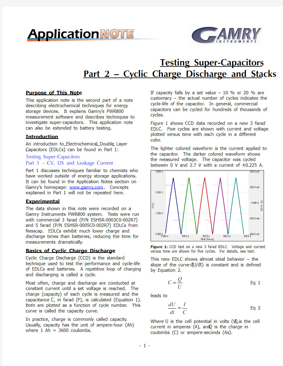
This application note is the second part of a note describing electrochemical techniques for energy storage devices. It explains Gamry’s PWR800 measurement software and describes techniques to investigate super-capacitors. This application note can also be extended to battery testing. If capacity falls by a set value – 10 % or 20 % are customary – the actual number of cycles indicates the cycle-life of the capacitor. In general, commercial capacitors can be cycled for hundreds of thousands of cycles. Figure 1 shows CCD data recorded on a new 3 farad EDLC. Five cycles are shown with current and voltage plotted versus time with each cycle in a different color. The lighter colored waveform is the current applied to the capacitor. The darker colored waveform shows the measured voltage. The capacitor was cycled between 0 V and 2.7 V with a current of ±0.225 A.
Introduction
An introduction to Electrochemical Double Layer Capacitors (EDLCs) can be found in Part 1:
Testing Super-Capacitors Part 1 – CV, EIS and Leakage Current
Part 1 discusses techniques familiar to chemists who have worked outside of energy storage applications. It can be found in the Application Notes section on Gamry’s homepage: https://www.360docs.net/doc/7011841130.html,. Concepts explained in Part 1 will not be repeated here.
Experimental
The data shown in this note were recorded on a Gamry Instruments PWR800 system. Tests were run with commercial 3 farad (P/N ESHSR-0003C0-002R7) and 5 farad (P/N ESHSR-0005C0-002R7) EDLCs from Nesscap. EDLCs exhibit much lower charge and discharge times than batteries, reducing the time for measurements dramatically.
Basics of Cyclic Charge Discharge
Cyclic Charge Discharge (CCD) is the standard technique used to test the performance and cycle-life of EDLCs and batteries. A repetitive loop of charging and discharging is called a cycle. Most often, charge and discharge are conducted at constant current until a set voltage is reached. The charge (capacity) of each cycle is measured and the capacitance C, in farad (F), is calculated (Equation 1). Both are plotted as a function of cycle number. This curve is called the capacity curve. In practice, charge is commonly called capacity. Usually, capacity has the unit of ampere-hour (Ah) where 1 Ah = 3600 coulombs. -1-
Figure 1: CCD test on a new 3 farad EDLC. Voltage and current versus time are shown for five cycles. For details, see text.
This new EDLC shows almost ideal behavior – the slope of the curve (dU/dt) is constant and is defined by Equation 2.
C=
leads to
Q U
Eq 1
dU I = dt C
Eq 2
Where U is the cell potential in volts (V), I is the cell current in amperes (A), and Q is the charge in coulombs (C) or ampere-seconds (As).
Figure 2 shows the same CCD procedure but on a 3 farad capacitor damaged by excessive voltage. This capacitor’s behavior is obviously far from ideal.
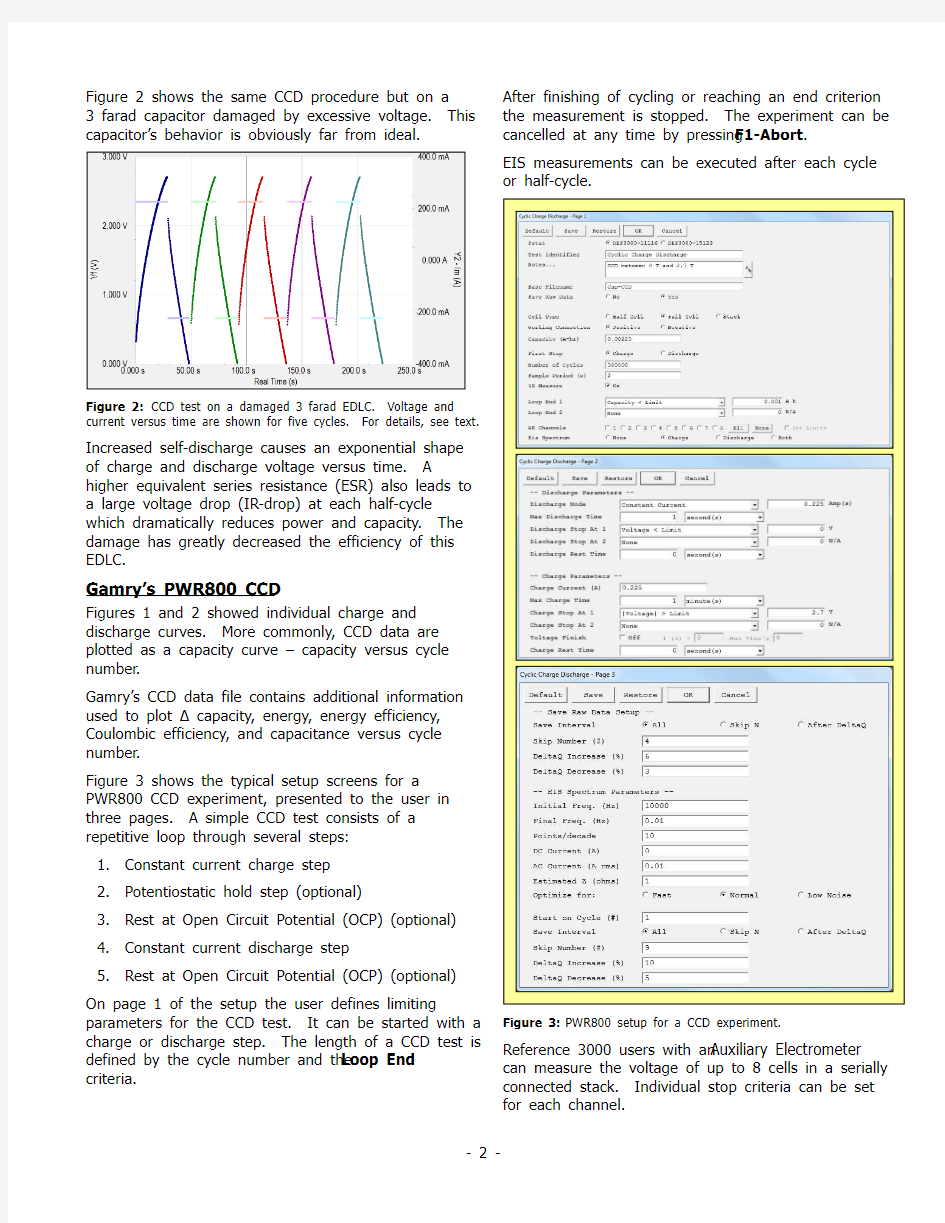
After finishing of cycling or reaching an end criterion the measurement is stopped. The experiment can be cancelled at any time by pressing F1-Abort. EIS measurements can be executed after each cycle or half-cycle.
Figure 2: CCD test on a damaged 3 farad EDLC. Voltage and current versus time are shown for five cycles. For details, see text.
Increased self-discharge causes an exponential shape of charge and discharge voltage versus time. A higher equivalent series resistance (ESR) also leads to a large voltage drop (IR-drop) at each half-cycle which dramatically reduces power and capacity. The damage has greatly decreased the efficiency of this EDLC.
Gamry’s PWR800 CCD
Figures 1 and 2 showed individual charge and discharge curves. More commonly, CCD data are plotted as a capacity curve – capacity versus cycle number. Gamry’s CCD data file contains additional information used to plot ? capacity, energy, energy efficiency, Coulombic efficiency, and capacitance versus cycle number. Figure 3 shows the typical setup screens for a PWR800 CCD experiment, presented to the user in three pages. A simple CCD test consists of a repetitive loop through several steps: 1. Constant current charge step 2. Potentiostatic hold step (optional) 3. Rest at Open Circuit Potential (OCP) (optional) 4. Constant current discharge step 5. Rest at Open Circuit Potential (OCP) (optional) On page 1 of the setup the user defines limiting parameters for the CCD test. It can be started with a charge or discharge step. The length of a CCD test is defined by the cycle number and the Loop End criteria.
Figure 3: PWR800 setup for a CCD experiment.
Reference 3000 users with an Auxiliary Electrometer can measure the voltage of up to 8 cells in a serially connected stack. Individual stop criteria can be set for each channel. -2-
Page 2 of the CCD setup (Figure 3) specifies the parameters for each charge and discharge step. The user selects the currents, voltage limits, and maximum time. The discharge process can be done in three different modes – Constant Current, Constant Power, or Constant Load. When a charge or discharge step reaches a stop criterion the loop continues with the next step. If Voltage Finish is enabled the charge step will proceed to a potentiostatic step. The Voltage Finish step ends after reaching a user specified time or when the current falls below a limiting value. The cell is turned off during an optional Rest Time period. After this period the cell is turned on again to proceed with the next step. Page 3 of the CCD setup in Figure 3 defines the save interval for the raw data (charge and discharge curves). This page also sets up EIS parameters for optional EIS experiments. After each loop the parameters for the capacity curve are calculated. Values are calculated for both charge and discharge steps. The cell is turned off when the experiment is finished.
Figure 4: Percentage change of capacity of a 3 farad EDLC by cycling to different voltage limits. 2.7 V, 3.1 V, 3.5 V, 4.0 V. For details, see text.
Capacity fade is more pronounced on the samples charged to higher voltage limits. The capacity is reduced by only 10 % after 50k cycles at potentials below 3.0 V. The capacitor charged to 4.0 V lost 20 % of its capacity after 500 cycles. The strong degradation of performance at higher potentials mainly occurs when Faradaic electrochemical reactions decompose the electrolyte. This can inhibit the electrode surface, lead to gas formation, damage the electrodes, and have other adverse effects.
CCD on Single 3 Farad EDLCs
Different voltage limits
Cycle-life depends on a number of variables: ? Limiting voltage, ? Current used for charge and discharge, ? Temperature To demonstrate the first point, four 3 farad EDLCs were cycled to different voltage limits – most of them well beyond the 2.7 V maximum voltage specified for the EDLC. Figure 4 shows the corresponding curves with the relative change of capacity for up to 50,000 (50k) cycles. The capacitors were charged and discharged with a current of ±2.25 amps. The lower voltage limit was 1.35 V which is the half rated voltage of the EDLC. The upper voltage limits were set to 2.7 V, 3.1 V, 3.5 V, and 4.0 V.
Different charge and discharge currents
Cycle-life also depends on the applied current. To demonstrate the impact of higher currents on CCD experiments, current values significantly beyond the specifications of the capacitor were chosen. The 3 F capacitors used in this application note are specified for 3.3 ampere currents. For these experiments currents larger than 3 A were needed. These currents require the use of a Gamry Instruments Reference 30k Booster. The Reference 30k Booster is an extension for the Reference 3000. Its compliance current is expanded to ±30 amperes. It works with all applications for the Reference 3000, including the Auxiliary Electrometer. For more information, visit Gamry’s website: https://www.360docs.net/doc/7011841130.html, Three capacity plots with different charge and discharge currents are shown in Figure 5. The EDLCs were charged and discharged between 1.35 V and 3.5 V. The applied current was set to 2.25 A, 7.5 A, and 15 A.
-3-
Table 1 shows that power loss is estimated to be greater than 2 watts, even at 7.5 A. The small 3 F capacitors used for these tests cannot dissipate this much power without getting very hot. The heat can cause degradation of the electrolyte and dramatically reduce life-time. The capacitor cycled at 15 A was so badly swollen at the end of the test that it was surprising it had not burst.
CCD on stacks for higher voltages
Balanced stack
Figure 5: Capacity curves of a 3 farad EDLC by cycling with 2.25 A, 7.5 A, 15 A. For details, see text. different currents.
The capacity curves at higher currents show a steep capacity decline with increasing cycle number. The two EDLCs that were cycled with 7.5 A and 15 A failed before reaching 400 and 800 cycles respectively. Even on the first CCD cycle, higher currents lead to reduced capacity. Voltage is lost due to IR-drop (ULoss) according to Equation 3:
For high-power applications several energy storage devices are often combined in serial and parallel circuits. For serially connected capacitors Equations 5 and 6 apply:
n 1 1 =∑ C i =1 Ci
n
Eq 5
U = ∑U i
i =1
Eq 6
U Loss = ESR ? I
Eq 3
The IR-drop voltage is not useful in charging and discharging the capacitor. Both charge and discharge have their effective voltage range Ueff reduced by twice the IR-drop voltage. Assuming 40 m ESR for 3 F capacitors, we’d expect these parameters for different currents:
The total capacity for n identical capacitors is the nth fraction of the capacity of a single capacitor. The individual voltages of the capacitors are summed to give the total voltage of the stack. Figure 6 shows a schematic diagram for a serially connected stack of capacitors.
I
[A] 2.25 7.5 15
ULoss
[V] 0.09 0.3 0.6
Ueff
[V] 1.97 1.55 0.95
Q
[mAh] 1.6 1.3 0.8
PLoss
[W] 0.2 2.3 9.0
Figure 6: Diagram of serially connected capacitors with Auxiliary Electrometer connections.
Table 1: Estimated IR-drop voltage, effective voltage range, capacity, and power loss for 3 F EDLCs with 40 m ESR. For details, see text.
If all single cells in a stack show the same parameters the stack is called balanced. The stack is unbalanced if there are cells that differ in performance parameters like capacitance, ESR, or leakage resistance. Gamry’s Auxiliary Electrometer enables detailed investigation of single cells in a stack. Each individual channel (AECH 1, AECH 2, AECH 3, …) measures the voltage across a cell. The Auxiliary Electrometer is currently supported in PWR800, EIS300, and the DC and AC Toolkits. For more information on the Auxiliary Electrometer option, visit Gamry’s website: https://www.360docs.net/doc/7011841130.html,
The IR-drop reduces capacity by about 19 % and 50 % respectively. Note the rough agreement between the initial capacities of the measurements with 7.5 A and 15 A in Figure 5 and Table 1. The two capacitors cycled with 7.5 A and 15 A got quite hot before they failed. The heat generated by rapid cycling is also due to IR-losses. Assuming a constant ESR, the power loss PLoss in these devices can be estimated from Equation 4:
PLoss = I 2 ? ESR
Eq 4 -4-
Capacity curves cannot show irregularities in stacks. All cells receive the same current so their capacities are identical. In the following sections, tests were done with small stacks containing three series-connected EDLCs. The stacks were deliberately unbalanced to show the impact of two common irregularities. To reveal these irregularities different plots were used.
small deviations from 1.3 V are probably due to leakage current imbalance, described later. The final charge voltage is more interesting. If we had a balanced stack, the fully-charged stack voltage of 9.5 V would be evenly divided among the cells so each cell would charge to about 3.16 V. In the unbalanced stack the 3 F EDLCs (C1 and C2) charge to around 3.36 V. They are each overcharged by about 200 mV. The 5 F capacitor (C3) is only charged to about 2.7 V. It is undercharged by 400 mV. Note the voltage imbalance is independent of the cycle number. In a capacitor stack with unbalanced capacitor values, the capacitors with the highest capacitances have a lower effective voltage range. These deviations in voltage also lead to differences in energy. Figure 8 shows the calculated energy of the charge step versus cycle number for the same measurement.
Unbalanced stack with different capacitances
Using capacitors with different capacitances in a stack leads to fluctuations in voltage defined by Equation 7.
Ui =
Q Ci
Eq 7
Applying a constant charge Q on a stack leads to a lower voltage Ui for single cells with higher capacitance Ci. A serial stack made up of two 3 farad EDLCs (C1, C2) and one 5 farad EDLC (C3) (see also Figure 6) was used to test an unbalanced stack. All three caps were initially charged to 1.35 V before being added to the stack, so the initial stack voltage was close to 4 V. The stack was cycled for 500 cycles with a current of ±0.225 A. The test started with a charge step. The cycle limits were set to 4 V and 9.5 V. Voltage of the single cells was measured with three Auxiliary Electrometer channels. Figure 7 shows one presentation of the data from this test. The limiting voltages of each channel for the charge (darker colored) and discharge step (lighter colored) versus cycle number are plotted.
Figure 8: Charge energy versus cycle number of single cells in an unbalanced stack with two 3 farad EDLCs ( C1, C2) and one 5 farad EDLC ( C3). For details, see text.
The energy of the 5 farad EDLC is reduced due to lower voltage limits. The two 3 farad EDLCs try to balance this voltage loss with higher voltages. Their energy content increased. In extreme cases, the voltage (and energy) increase can be large enough to damage the capacitors.
Unbalanced stack with different leakage resistances
Leakage resistance affects both stack performance and cycle-life. It can change as a capacitor ages. Low leakage resistances lead to higher leakage currents which discharge the cell without external current applied. Leakage resistance can be modeled as a resistor parallel to a capacitor (see Figure 9).
Figure 7: Limiting potentials for the charge (darker) and discharge process (lighter) of an unbalanced stack with two 3 farad EDLCs ( C1, C2) and one 5 farad EDLC ( C3). For details, see text.
As expected, the final discharge voltage for each cell (regardless of capacitance) is close to 1.3 V. The
-5-
Higher leakage currents also lead to increased loss in energy and power. Figure 11 shows the behavior of energy during cycling. The prior stack setup was cycled for 500 cycles between 4 V and 8.1 V with a current of ±0.225 A.
Figure 9: Diagram of serially connected capacitors with Auxiliary Electrometer connections. Parallel resistors R1 and R2 simulate different leakage resistances.
Figure 10 shows the self-discharge due to leakage current. Two resistors (R1 = 16.5 k , R2 = 154 k ) were installed parallel to C1 and C2 (3 F). The intrinsic leakage resistance for C3 (3 F) is in the M -range. The stack was charged to 8.1 V using a charge current of 0.225 A. After charging to 8.1 V the voltage was recorded in currentless state for 6 hrs.
Figure 11: Charge energy versus cycle number of single cells ( C1, C2, C3) with different leakage resistances in an unbalanced stack. For details, see text.
Higher leakage currents cause continuous energy fade during cycling. Energy of C1 decreases continuously due to higher self-discharge. Note this is in contrast to Figure 7 and Figure 8 where voltage and energy imbalances were independent of the cycle number. Capacitors C2 and C3 compensate for this loss and overcharge to higher voltages. Energy increases but this may be at the cost of lower electrochemical stability and decreased cycle-life.
Figure 10: Self-discharge over 6 hrs of an unbalanced stack ( ) and its single cells ( C1, C2, C3) with different leakage resistances. For details, see text.
Conclusion
This application note described Gamry’s PWR800 CCD software by measurements on single 3 F EDLCs and small stacks. Impacts of different setup parameters on performance of EDLCs were shown and the influence of common irregularities in stacks was described. The combination of single-cell investigation and recording of multiple parameters enables accurate evaluation of irregularities in stacks.
Internal leakage current leads to a continuous voltage drift that discharges the cell. Capacitor C1 with the lowest leakage resistance has the highest leakage current. It causes the highest loss in voltage (about 850 mV). In comparison, the total voltage loss of the stack is about 1 V after 6 hrs. The calculated leakage current for C1 is 47 A. The other capacitors exhibit leakage currents of only 7 A (C2) and 2 A (C3). This measurement was done with a special Self-discharge script that was added to the PWR800 software (Revision 5.61 and newer) and is named: PWR Self-Discharge.exp
Testing Super-Capacitors, Part 2 – Cyclic Charge Discharge and Stacks. Rev 1.0 11/14/2011 ? Copyright 1990 – 2011 Gamry Instruments, Inc.
734 Louis Drive ? Warminster, PA 18974, USA ? Tel. (215) 682-9330 ? Fax (215) 682-9331 ? https://www.360docs.net/doc/7011841130.html, ? info@https://www.360docs.net/doc/7011841130.html,
-6-