32415ASQM4G03T中文资料
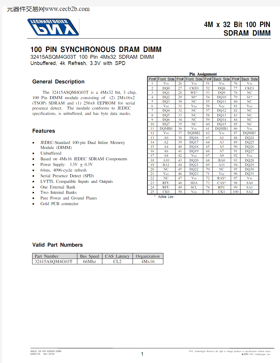

Pin Assignment
Pin#Front Side Pin#Front Side Pin#Back Side Pin#Back Side 1Vss 26Vss 51Vss 76Vss 2DQ027CKE052DQ877CKE13DQ128WE*53DQ978NC 4DQ229S0*54DQ1079S1*5DQ330NC 55DQ1180NC 6Vcc 31Vcc 56Vcc 81Vcc 7DQ432NC 57DQ1282NC 8DQ533NC 58DQ1383NC 9DQ634NC 59DQ1484NC 10DQ735NC 60DQ1585NC 11DQMB036Vss 61DQMB186Vss 12Vss 37DQMB262Vss 87DQMB313A038DQ1663A188DQ2414A239DQ1764A389DQ2515A440DQ1865A590DQ2616A641DQ1966A791DQ2717A842Vcc 67A992Vcc 18A1043DQ2068BA093DQ2819BA144DQ2169A1194DQ2920NC 45DQ2270NC 95DQ3021Vcc 46DQ2371Vcc 96DQ3122NC 47Vss 72RAS*97Vss 23RFU 48SDA 73CAS*98SA024RFU 49SCL 74RFU 99SA125CK050Vcc 75CK1100SA2 * Active Low
100 PIN SYNCHRONOUS DRAM DIMM
32415ASQM4G03T 100 Pin 4Mx32 SDRAM DIMM Unbuffered, 4k Refresh, 3.3V with SPD
Features
? JEDEC-Standard 100-pin Dual Inline Memory
Module (DIMM)? Unbuffered
? Based on 4Mx16 JEDEC SDRAM Components ? Power Supply: 3.3V ± 0.3V ? 64ms, 4096-cycle refresh ? Serial Presence Detect (SPD)
? LVTTL Compatible Inputs and Outputs ? One External Bank ? Two Internal Banks
? Pure Power and Ground Planes ? Gold PCB connector
General Description
The 32415ASQM4G03T is a 4Mx32 bit, 3 chip,100 Pin DIMM module consisting of (2) 2Mx16x2(TSOP) SDRAM and (1) 256x8 EEPROM for serial presence detect. The module conforms to JEDEC specifications, is unbuffered, and has byte data masks.
Valid Part Numbers
Part Number
Bus Speed CAS Latency
Organization 32415ASQM4G03T
66Mhz
CL2
4Mx16
Block Diagram
Pin Descriptions
Pin Name Function
CLK#System Clock All input signals are sampled on the rising edge of clock.
S#Chip Select Enables and disables the command decoder. All commands are disabled
when S# is high.
CKE Clock Enable Masks system clock to freeze current operation on the next clock cycle,
also provides access to standby mode (see truth table).
A#Address Lines Input lines for Row/Column address.
BA#Bank Select Lines Selects the internal bank to be accessed during a row or column address
latch.
RAS Row Address Strobe Latches the row address on the rising edge of clock when asserted. CAS Column Address Strobe Latches the column address on the rising edge of clock when asserted. WE Write Enable Enables write operation and row precharge.
DQMB#Data Masks Provides a byte mask for write operations and a byte enable for read
operations.
DQ#Data Lines Data input/output lines.
Vdd Power Supply Power Supply 3.3V±0.3V
Vss Ground Ground
SDA, SCL SPD Data/Clock Lines Serial Presence Detect (SPD) EEPROM bus lines. These line provides
bi-directional data transfer over an I2C bus.
SA#SPD Address Lines Serial Presence Detect (SPD) EEPROM address lines. These lines are
used to configure the SPD.
NC No Connection Line is not connected in DIMM.
Serial Presence Detect Matrix
Byte #Function
Description
Binary Hex
76543210MS-LS
0Define # of bytes written into EEPROM1000000080128
1Total # of bytes of SPD memory device0000100008256
2Fundamental memory type (EDO,SDRAM...)0000010004SDRAM
3# of row addresses000011000C12
4# of column addresses00001000088
5# of module rows00000001011
6Data width (001000002032)
7...Data width continued000000000000
8Voltage interface0000000101LVTTL
9SDRAM cycle time10100000A010ns
10SDRAM access from clock10000000808ns
11DIMM configuration type (non-parity,ECC…)0000000000non-parity 12Refresh rate/type1000000080Normal/Self 13Primary SDRAM width000100001016
14Error checking SDRAM width00000000000
15Minimum clock delay back to back random column address00000001011
16Burst lengths supported100011118F page/8/4/2/1 17# of banks on each SDRAM device00000100044
18CAS# latencies supported00000110063/2
19CS# latency0000000101CS latency=0 20Write latency0000000101WE latency=0 21SDRAM module attributes0000000000Unbuffered 22SDRAM device attributes: general000011100E Write1/Read burst/Precharge 23Min SDRAM cycle time at CL X-110010000909ns
24SDRAM access from clock at CL X-110000000808ns
25Min SDRAM cycle time at CL X-2000000000000
26Max SDRAM access from clock at CL X-2000000000000
27Min row precharge time000110101A26ns
28Min row active to row active000101001420ns
29Min RAS to CAS delay000110101A26ns
30Minimum RAS pulse width001100103250ns
31Density of each row on module000001000432MB 32-61Superset information (may be used in future)000000000000
62SPD data revision code0001001012 1.2
63Checksum for bytes 0-6210111100BC188 64-125Manufacturer's information0000000000Not written 126Intel specification frequency011001106666Mhz 127Intel specification CAS# latency support1000011086CAS latency 2
128-255Unused storage locations0000000000Not written NOTE: 1. x = Variable Data.
Simplified Truth Table
Command
CKEn-1CKEn CS RAS CAS WE DQM BA
A10/AP
A11,A9-A0
Note Register Mode Register Set H X L L L L X Mode Register Data
1
Auto refresh
H Entry H L L L L H X X
Refresh
Self
Refresh Exit
L H H X X X X X
Bank active & row addr.H X L L H H X V Row Address Auto precharge disable L Read &column address Auto precharge
enable
H
X
L
H
L
H
X
V
H Column
address
2
Auto precharge disable L Write &column address Auto precharge
enable
H X L H L L X V
H
Column address
2
Bank Selection V L Prechar ge All Banks H X L L H L X X
H X Entry H L H X X X X Clock Suspend or active power down Exit L H
H
X X
X
X X DQM
H
X
V
X
3
Notes:
1. MRS can be issued only in idle state.
2. A burst read or write with auto precharge cannot be interrupted. New commands can be issued Trp after the end of the burst
3. DQM sampled on positive clock edge results in Hi-Z within 2 cycles, however data is immediately invalid and should be ignored.
Absolute Maximum Ratings
Parameter Symbol Value Units
Voltage on any pin relative to Vss V in-0.5 to 4.6V
Short circuit output current I out50mA
Power dissipation Pt2W
Operating temperature T opr0 to +70°C
Storage temperature T st-55 to +125°C
NOTE: Permanent damage may occur if absolute maximum ratings are exceeded.
Device should be operated within recommended operating conditions only.
DC Characteristics (T A = 0 to 70C, Vcc = 3.3V ± 0.3V)
Parameter Symbol Min Typ Max Units Note Supply voltage V SS000V
Supply voltage V CC 3.0 3.3 3.6V
Input high voltage V IH 2.0-Vcc+0.3V1 Input low voltage V IL-0.3-0.8V2 Output high voltage V OH 2.4--V I OH=-2mA Output low voltage V OL--0.8V I OL=2mA
DQm.CBm-1-+1μA
SDA,SCL,
SAm,CKEm
-10-+10μA
CKm,Sm-2-+2μA
RAS*,CAS*, WE*,Am,BA0-2-+2μA
Leakage Current
DQMBm I IL
-1-+1μA
DC Current Consumption (T A = 0 to 70C, Vcc = 3.3V ± 0.3V)
Parameter Symbol Test Condition Current Unit Note Operating Current I CC1Burst Length = 1, t RC > t RC (min) , I OL = 0 mA160mA3, 4 Operating Current , Burst mode (CL= 3)I CC4BL = 4 , I OL= 0Ma, Tck = Min330mA3, 4, 5 Operating Current , Burst mode (CL= 2)I CC4BL = 4 , I OL= 0Ma, Tck = Min260mA3, 4, 5 Refresh Current , 4K refresh I CC5t RC > t RC (min)260mA3 Self Refresh Current I CC6CKE < 0.2 V2mA3 CL : CAS Latency
Capacitance (T A = 0 to 70C, Vcc = 3.3V ± 0.3V, Vss = 0V)
Parameter Symbol Typ Max Units Note Input capacitance (Am, BA0,CKEm)C I1-8pF
Input capacitance (DQMBm)C I2-4pF
Input capacitance (CAS*, RAS*, WE*)C I3-8pF
Input capacitance (CKm)C I4-8pF
Input capacitance (SDA,SCL,SAm)-10pF
Input/Output capacitance (DQm,CBm)C I/O- 6.5pF
AC Characteristics (T A = 0 to 70C, Vcc = 3.3V ± 0.3V, Vss = 0V)
Parameter Symbol
Units Note
Time
Min Max
CLK Cycle time (CL =3)t CK101000ns6,7 CLK Cycle time (CL =2)t CK151000ns6,7 CLK Cycle time (CL =1)t CK301000ns6,7 CLK to valid output delay (CL =3)t AC-8ns6,7 CLK to valid output delay (CL =2)t AC-12ns 6.7 CLK to valid output delay (CL =1)t AC-27ns 6.7 Output data hold time t OH3-ns7 Output valid to High-Z t HZ3-ns7 CLK high pulse width t CH3-ns7 CLK low pulse width t CL3-ns7 Command setup time t CMS3-ns7 Address setup time t AS3-ns7 Clock enable setup time t CKS3-ns7 Data input setup time t DS3-ns7 Command hold time t CMH1-ns7 Address hold time t AH1-ns7 Clock enable hold time t CKH1-ns7 Data input hold time t DH1-ns7 Power down exit setup time t PDE1-ns7,8 CLK to output in Low-Z t LZ1-ns7 Row active to Row active delay t RRD (min)20-ns6 RAS* to CAS* delay t RCD (min)20-ns6 Row precharge time t RP (min)20-ns6 Row active time t RAS (min)50-ns6 Row active time t RAS (max)8-us
Row cycle time t RC (min)70-ns6 Mode Register set to Active Delay t RSC (min)30-ns
CL : CAS Latency
Notes :
1.Overshoot: Vih (MAX) = Vdd +
2.0V for ≤3ns
2.Undershoot: Vil (MIN) = Vss – 2.0V for ≤3ns
3.Typical peak current consumption.
4.Measured with outputs open.
5.Assumes minimum column address update cycle: t CCD(min).
6.Parameters depend on programmed CAS Latency.
7.Assumed input rise and fall time=1ns.
8. A time of t PDE has to elapse after asserting CKE to resume normal operation when exiting power down mode.
Timings listed are for discrete SDRAM components.
CLK
t AH
t AS
t CH t CK
t CKS
t CL t T
t CMS
t T
t CMH
t
CMH
t CMS t
CMH
t CMS t CMH
t CMS t CMH
t CMS t CKH
t CKS t CKS
t CKH
t
CKH
V IH V IL
CS
RAS
CAS
WE
A0-A11BS0,1
CKE
Command Input Timing
t AC DQ
Read Command
t LZ
t OH
t AC
t OH
t HZ
Burst Length
VALID DATA OUT
VALID DATA OUT
CS
RAS
WE
CAS
CLK
A0-A1BS0,1
CAS Read Latency
Read Timing
CKE
CLK
DQM
VALID DATA IN
VALID DATA IN VALID DATA IN VALID DATA IN
VALID DATA IN
VALID DATA IN
VALID DATA IN
VALID DATA IN
DQ0~7
CLK
DQ0~7
(Clock Mask)
(Word Mask)
Control Timing of Input Data
t CMH
t CKS t
CKH
t DH
t DS
t DS
t DS
t DH
t DH
t DH
t DS
t CKS
t CKH
t DS
t DH
t DH
t DH
t DH
t DS
t DS
t DS
t CMH
t CMS t CMS
t AC
t AC
t CMH
t CKH
t OH
t HZ
t LZ t OH
t OH t OH
t OH
t AC
t AC
t CMS t CMH t CMS t AC
t AC
t OH
t OH
t OH
t AC
t AC
t CKS t CKH
t CKS CLK
DQM
DQ0~7CLK
CKE
DQ0~7
(Clock Mask)
(Output Enable)
Control Timing of Output Data VALID DATA OUT VALID DATA OUT
VALID DATA OUT
VALID DATA OUT
VALID DATA OUT
VALID DATA OUT
t RSC
t CMH
t CMS t CMH
t CMS t CMH
t CMS t CMH
t CMS t AH
t AS
Register Set Data
Next Command
CLK
CS
RAS
CAS
WE
A0 to A10
BS
Mode Register Set Cycle