RF2361 PCBA-L中文资料
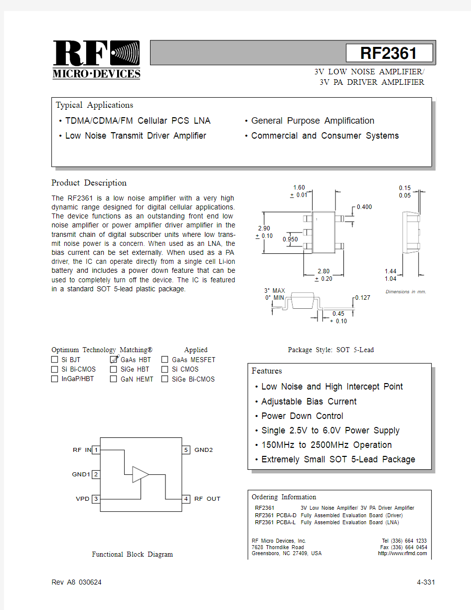
Product Description
Ordering Information
Typical Applications
Features
Functional Block Diagram
RF Micro Devices, Inc.7628 Thorndike Road
Greensboro, NC 27409, USA
Tel (336) 664 1233Fax (336) 664 0454https://www.360docs.net/doc/989952605.html,
Optimum Technology Matching? Applied
Si BJT GaAs MESFET GaAs HBT
Si Bi-CMOS SiGe HBT
Si CMOS InGaP/HBT
GaN HEMT
SiGe Bi-CMOS
VPD GND2
RF OUT
3V LOW NOISE AMPLIFIER/3V PA DRIVER AMPLIFIER
?TDMA/CDMA/FM Cellular PCS LNA ?Low Noise Transmit Driver Amplifier
?General Purpose Amplification ?Commercial and Consumer Systems
The RF2361 is a low noise amplifier with a very high dynamic range designed for digital cellular applications.The device functions as an outstanding front end low noise amplifier or power amplifier driver amplifier in the transmit chain of digital subscriber units where low trans-mit noise power is a concern. When used as an LNA, the bias current can be set externally. When used as a PA driver, the IC can operate directly from a single cell Li-ion battery and includes a power down feature that can be used to completely turn off the device. The IC is featured in a standard SOT 5-lead plastic package.
?Low Noise and High Intercept Point ?Adjustable Bias Current ?Power Down Control
?Single 2.5V to 6.0V Power Supply ?150MHz to 2500MHz Operation ?Extremely Small SOT 5-Lead Package
RF23613V Low Noise Amplifier/ 3V PA Driver Amplifier RF2361 PCBA-D Fully Assembled Evaluation Board (Driver)RF2361 PCBA-L Fully Assembled Evaluation Board (LNA)+ 0.10
Package Style: SOT 5-Lead
!
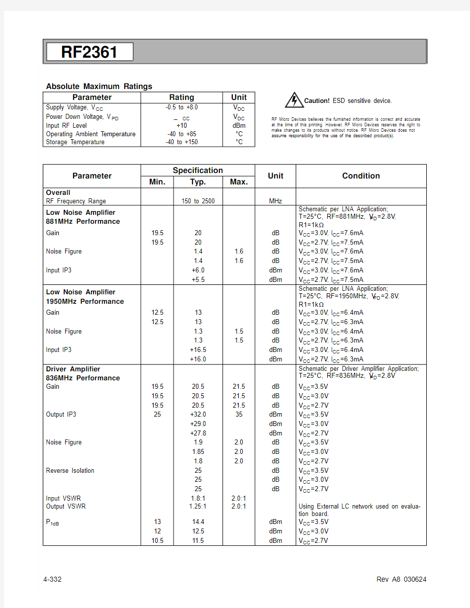
Absolute Maximum Ratings
Parameter
Rating
Unit
Supply Voltage, V CC
-0.5 to +8.0V DC Power Down Voltage, V PD +10dBm Operating Ambient T emperature -40 to +85°C Storage Temperature -40 to +150 °C Parameter Specification Unit Condition Min.Typ.Max. Overall RF Frequency Range 150 to 2500 MHz Low Noise Amplifier 881MHz Performance Schematic per LNA Application;T=25°C, RF=881MHz, V PD =2.8V , R1=1k ? Gain 19.520dB V CC =3.0V , I CC =7.6mA 19.5 20dB V CC =2.7V , I CC =7.5mA Noise Figure 1.4 1.6dB V CC =3.0V , I CC =7.6mA 1.4 1.6 dB V CC =2.7V , I CC =7.5mA Input IP3 +6.0dBm V CC =3.0V , I CC =7.6mA +5.5 dBm V CC =2.7V , I CC =7.5mA Low Noise Amplifier 1950MHz Performance Schematic per LNA Application; T=25°C, RF=1950MHz, V PD =2.8V , R1=1k ? Gain 12.513dB V CC =3.0V , I CC =6.4mA 12.5 13dB V CC =2.7V , I CC =6.3mA Noise Figure 1.3 1.5dB V CC =3.0V , I CC =6.4mA 1.3 1.5 dB V CC =2.7V , I CC =6.3mA Input IP3 +16.5dBm V CC =3.0V , I CC =6.4mA +16.0 dBm V CC =2.7V , I CC =6.3mA Driver Amplifier 836MHz Performance Schematic per Driver Amplifier Application;T=25°C, RF=836MHz, V PD =2.8V Gain 19.520.521.5dB V CC =3.5V 19.520.521.5dB V CC =3.0V 19.520.521.5dB V CC =2.7V Output IP3 25 +32.035 dBm V CC =3.5V +29.0dBm V CC =3.0V +27.8dBm V CC =2.7V Noise Figure 1.9 2.0dB V CC = 3.5V 1.85 2.0dB V CC =3.0V 1.8 2.0 dB V CC =2.7V Reverse Isolation 25dB V CC =3.5V 25dB V CC =3.0V 25dB V CC =2.7V Input VSWR 1.8:1 2.0:1Output VSWR 1.25:1 2.0:1 Using External LC network used on evalua-tion board.P 1dB 1314.4dBm V CC =3.5V 1212.5dBm V CC =3.0V 10.5 11.5 dBm V CC =2.7V ESD sensitive device. RF Micro Devices believes the furnished information is correct and accurate at the time of this printing. However, RF Micro Devices reserves the right to make changes to its products without notice. RF Micro Devices does not assume responsibility for the use of the described product(s). Parameter Specification Unit Condition Min.Typ.Max. Power Supply T=25 °C Voltage (V CC) 2.5 to 6.0V Voltage (V PD) 2.7 2.8 2.9V Current Consumption - Driver Amplifier 12.521.527mA V CC=3.5V; V PD=2.8V; V PD+V CC - Current Consumption from V PD is 2.0mA T yp. @ V PD=2.8V and 3.0mA Max @ V PD=2.9V 182022mA V CC=3.5V; V PD=2.7V; V PD+ V CC 192329mA V CC=3.5V; V PD=2.9V; V PD+ V CC Power Down 10μA V CC=3.5V; V PD≤0.9V Driver Amplifier 1880MHz Performance Schematic per Driver Amplifier Application; T=25°C, RF=1880MHz, V PD=2.8V Gain13.014.014.5dB V CC=3.5V 13.014.014.5dB V CC=3.0V 13.014.014.5dB V CC=2.7V Output IP327+35.038dBm V CC=3.5V +31.0dBm V CC=3.0V +28.8dBm V CC=2.7V Noise Figure 1.85 2.0dB V CC=3.5V 1.8 2.0dB V CC= 3.0V 1.75 2.0dB V CC=2.7V Reverse Isolation19dB V CC=3.5V 19dB V CC=3.0V 19dB V CC=2.7V Input VSWR 1.6:1 2.0:1 Output VSWR 1.6:1 2.0:1Using External LC network used on evalua- tion board. P1dB1415.6dBm V CC=3.5V 1314.1dBm V CC=3.0V 1213.1dBm V CC=2.7V Power Supply T=25 °C Voltage (V CC) 2.5 to 6.0V Voltage (V PD) 2.7 2.8 2.9V Current Consumption - Driver Amplifier 11.519.525.5mA V CC=3.5V; V PD=2.8V; V PD+V CC - Current Consumption from V PD is 2.0mA T yp.@ V PD=2.8V and 3.0mA Max @ V PD=2.9V 161820mA V CC=3.5V; V PD=2.7V; V PD+ V CC 1820.527mA V CC=3.5V; V PD=2.9V; V PD+ V CC Power Down 10μA V CC=3.5V; V PD≤0.9V Application Schematic: Low Noise Amplifier ~881MHz Operation Application Schematic: Low Noise Amplifier ~1950MHz Operation J1J2 RF OUT J1J2 RF OUT Application Schematic: Driver Amplifier ~836MHz Operation Application Schematic: Driver Amplifier ~1880MHz Operation J1J2RF OUT VCC J1J2RF OUT Evaluation Board Schematic: Low Noise Amplifier ~881MHz Operation (Download Bill of Materials from https://www.360docs.net/doc/989952605.html,.) Evaluation Board Schematic:Driver Amplifier ~836MHz Operation J1 J2 RF OUT VCC J1 J2 RF OUT VCC Evaluation Board Layout - 900MHz Driver Board Size 0.948” x 1.063” Board Thickness 0.031”; Board Material FR-4 Evaluation Board Layout - 900MHz LNA PCB Design Requirements PCB Surface Finish The PCB surface finish used for RFMD's qualification process is electroless nickel, immersion gold. T ypical thickness is 3μinch to 8μinch gold over 180μinch nickel. PCB Land Pattern Recommendation PCB land patterns are based on IPC-SM-782 standards when possible. The pad pattern shown has been developed and tested for optimized assembly at RFMD; however, it may require some modifications to address company specific assembly processes. The PCB land pattern has been developed to accommodate lead and package tolerances. PCB Metal Land Pattern A = 0.70 x 1.00 (mm) Typ. Dimensions in mm. Figure 1. PCB Metal Land Pattern (Top View) PCB Solder Mask Pattern Liquid Photo-Imageable (LPI) solder mask is recommended. The solder mask footprint will match what is shown for the PCB metal land pattern with a 2mil to 3mil expansion to accommodate solder mask registration clearance around all pads. The center-grounding pad shall also have a solder mask clearance. Expansion of the pads to create solder mask clearance can be provided in the master data or requested from the PCB fabrication supplier. A = 0.90 x 1.20 (mm) Typ. Dimensions in mm. Figure 2. PCB Solder Mask (Top View)