M38239G4-XXXHP中文资料
DESCRIPTION
The 3823 group is the 8-bit microcomputer based on the 740 fam-ily core technology.
The 3823 group has the LCD drive control circuit, an 8-channel A/ D converter, a serial interface, a watchdog timer, a ROM correc-tion function, and as additional functions.
The various microcomputers in the 3823 group include variations of internal memory size and packaging. For details, refer to the section on part numbering.
FEATURES
●Basic machine-language instructions (71)
●The minimum instruction execution time...........................0.4 μs (at f(X IN) = 10 MHz, High-speed mode)
●Memory size ROM...............................................................16 K to 60 K bytes RAM.................................................................640 to 2560 bytes ●ROM correction function..............................32 bytes ? 2 blocks ●Watchdog timer..............................................................8-bit ? 1●Programmable input/output ports.. (49)
●Input ports (5)
●Software pull-up/pull-down resistors (Ports P0-P7 except port P40)●Interrupts.................................................17 sources, 16 vectors
(includes key input interrupt)●Key Input Interrupt (Key-on Wake-Up) (8)
●Timers...........................................................8-bit ? 3, 16-bit ? 2●Serial interface............8-bit ? 1 (UART or Clock-synchronized)●A/D converter............10-bit ? 8 channels or 8-bit ? 8 channels ●LCD drive control circuit Bias...................................................................................1/2, 1/3 Duty...........................................................................1/2, 1/3, 1/4 Common output.. (4)
Segment output (32)
●Main clock generating circuits..............Built-in feedback resistor
(connect to external ceramic resonator or quartz-crystal oscillator)●Sub-clock generating circuits
(connect to external quartz-crystal oscillator or on-chip oscillator)●Power source voltage
In frequency/2 mode (f(X IN) ≤ 10 MHz)...................4.5 to 5.5 V In frequency/2 mode (f(X IN) ≤ 8 MHz).....................4.0 to 5.5 V In frequency/4 mode (f(X IN) ≤ 10 MHz)...................2.5 to 5.5 V In frequency/4 mode (f(X IN) ≤ 8 MHz).....................2.0 to 5.5 V In frequency/4 mode (f(X IN) ≤ 5 MHz).....................1.8 to 5.5 V In frequency/8 mode (f(X IN) ≤ 10 MHz)...................2.5 to 5.5 V In frequency/8 mode (f(X IN) ≤ 8 MHz).....................2.0 to 5.5 V In frequency/8 mode (f(X IN) ≤ 5 MHz).....................1.8 to 5.5 V In low-speed mode....................................................1.8 to 5.5 V ●Power dissipation
In frequency/2 mode...............................................18 mW (std.) (at f(X IN) = 8 MHz, Vcc = 5 V, Ta = 25 °C)
In low-speed mode at X CIN................................................18 μW (std.) (at f(X IN) stopped, f(X CIN) = 32 kHz, Vcc = 2.5 V, Ta = 25 °C)
In low-speed mode at on-chip oscillator..................35 μW (std.) (at f(X IN) stopped, f(X CIN) = stopped, Vcc = 2.5 V, Ta = 25 °C)
●Operating temperature range..................................– 20 to 85 °C APPLICATIONS
Camera, audio equipment, household appliances, consumer elec-tronics, etc.
3823 Group
SINGLE-CHIP 8-BIT CMOS MICROCOMPUTER REJ03B0146-0202
Rev.2.02
Jun.19.2007
Table 1 Performance overview
Parameter
71
0.4 μs (Minimum instruction, f(X IN ) 10 MHz, High-speed mode)10 MHz (Maximum)16 K to 60 K bytes 640 to 2560 bytes 4-bit ? 1, 1-bit ? 1(4 pins sharing SEG)8-bit ? 5, 7-bit ? 1, 2 bit ? 1(16 pins sharing SEG)
17 sources, 16 vectors (includes key input interrupt)8-bit ? 3, 16-bit ? 2
8-bit ? 1 (UART or Clock-synchronized)10-bit ? 8 channels or 8 bit ? 8 channels 8-bit ? 1
32 bytes ? 2 blocks 1/2, 1/32, 3, 4432
Built-in feedback resistor
(connect to external ceramic rasonator or quartz-crystal oscillator)Built-in feedback resistor
(connect to external quartz-crystal oscillator or on-chip oscillator)4.5 to 5.5V 4.0 to 5.5V 2.5 to 5.5V 2.0 to 5.5V 1.8 to 5.5V 2.5 to 5.5V 2.0 to 5.5V 1.8 to 5.5V 1.8 to 5.5V
Std. 18 mW (Vcc = 5V, f(X IN ) = 8MHz, Ta = 25 °C)
Std. 18 μW (Vcc = 2.5V, f(X IN ) = stopped, f(X CIN ) = 32kHz, Ta = 25 °C)Std. 35 μW (Vcc = 2.5V, f(X IN ) = stopped, f(X CIN ) = stopped, Ta = 25 °C)V CC 10mA -20 to 85 °C CMOS sillicon gate
80-pin plastic molded LQFP/QFP
Number of basic instructions Instruction execution time Oscillation frequency Memory sizes ROM RAM Input port P34-P37, P40
I/O port P0-P2, P41-P47, P5, P6, P70, P71
Interrupt Timer
Serial interface A/D converter Watchdog timer ROM correction function LCD drive control Bias circuit
Duty
Common output Segment output
Main clock generating circuits Sub-clock generating circuits Power source voltage
In frequency/2 mode (f(X IN ) ≤ 10MHz)In frequency/2 mode (f(X IN ) ≤ 8MHz)In frequency/4 mode (f(X IN ) ≤ 10MHz)In frequency/4 mode (f(X IN ) ≤ 8MHz)In frequency/4 mode (f(X IN ) ≤ 5MHz)In frequency/8 mode (f(X IN ) ≤ 10MHz)In frequency/8 mode (f(X IN ) ≤ 8MHz)In frequency/8 mode (f(X IN ) ≤ 5MHz)In low-speed mode
Power dissipation
In frequency/2 mode In low-speed mode at X CIN
In low-speed mode at on-chip oscillator
Input/Output Input/Output withstand voltage characteristics
Output current Operating temperature range Device structure Package
Function
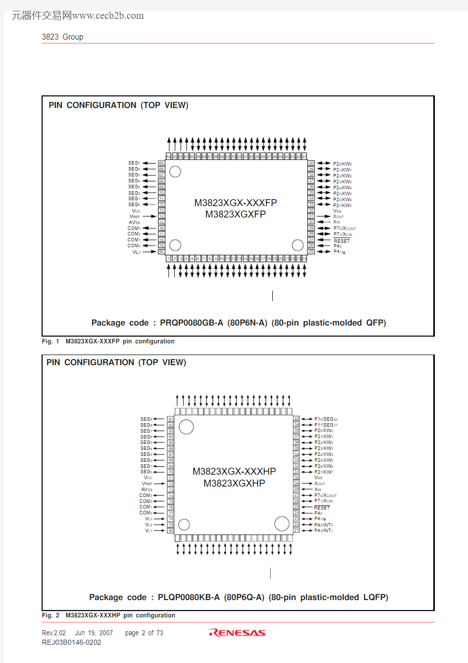
PIN DESCRIPTION
Table 2 Pin description (1)
V CC , V SS Function
Pin Name Function except a port function
?LCD segment output pins
Power source ?Apply voltage of power source to V CC , and 0 V to V SS . (For the limits of V CC , refer to “Recom-mended operating conditions”).
V REF AV SS RESET X IN X OUT
V L1–V L3COM 0–COM 3
SEG 0–SEG 11P00/SEG 16–P07/SEG 23
P10/SEG 24–P17/SEG 31P20/KW 0 –P27/KW 7
P34/SEG 12 –P37/SEG 15
Analog refer-ence voltage Analog power source Reset input Clock input Clock output
LCD power source
Common output
Segment output I/O port P0
I/O port P1
I/O port P2
?Reference voltage input pin for A/D converter.?GND input pin for A/D converter.?Connect to V SS .
?Reset input pin for active “L”.
?Input and output pins for the main clock generating circuit.?Feedback resistor is built in between X IN pin and X OUT pin.
?Connect a ceramic resonator or a quartz-crystal oscillator between the X IN and X OUT pins to set the oscillation frequency.
?If an external clock is used, connect the clock source to the X IN pin and leave the X OUT pin open.?This clock is used as the oscillating source of system clock.
?Input 0 ≤ V L1 ≤ V L2 ≤ V L3 voltage.?Input 0 – V L3 voltage to LCD.?LCD common output pins.
?COM 2 and COM 3 are not used at 1/2 duty ratio.?COM 3 is not used at 1/3 duty ratio.
?LCD segment output pins.?8-bit I/O port.
?CMOS compatible input level.?CMOS 3-state output structure.
?I/O direction register allows each port to be individually programmed as either input or output.?Pull-down control is enabled.?8-bit I/O port.
?CMOS compatible input level.?CMOS 3-state output structure.
?I/O direction register allows each pin to be individually programmed as either input or output.?Pull-up control is enabled.
?4-bit input port.
?CMOS compatible input level.?Pull-down control is enabled.
?Key input (key-on wake-up) interrupt input pins
?LCD segment output pins
Input port P3
Table 3 Pin description (2)
Function
Pin Function except a port function P40P42/INT 0,P43/INT 1P44/R X D,P45/T X D,P46/S CLK ,
P47/S RDY /S OUT
P50/INT 2,
P51/INT 3P52/RTP 0,P53/RTP 1P54/CNTR 0,P55/CNTR 1P56/T OUT P57/ADT P60/AN 0–P67/AN 7
P70/X COUT,P71/X CIN
?1-bit Input port.
?CMOS compatible input level.?7-bit I/O port.
?CMOS compatible input level.?CMOS 3-state output structure.
?I/O direction register allows each pin to be individually programmed as either input or output.?Pull-up control is enabled.?8-bit I/O port.
?CMOS compatible input level.?CMOS 3-state output structure.
?I/O direction register allows each pin to be individually programmed as either input or output.?Pull-up control is enabled.
?8-bit I/O port.
?CMOS compatible input level.?CMOS 3-state output structure.
?I/O direction register allows each pin to be individually programmed as either input or output.?Pull-up control is enabled.
?2-bit I/O port.
?CMOS compatible input level.?CMOS 3-state output structure.
?I/O direction register allows each pin to be individually programmed as either input or output.?Pull-up control is enabled.
?φ clock output pin ?Interrupt input pins
?Interrupt input pins ?Real time port function pins ?Timer X, Y function pins ?Timer 2 output pins ?A/D conversion input pins ?Sub-clock generating circuit I/O pins.(Connect a resonator. External clock cannot be used.)P41/φ
?Serial interface function pins
?A/D trigger input pins
Name I/O port P4
I/O port P5I/O port P6
I/O port P7
Input port P4?QzROM program power pin
PART NUMBERING
Fig. 4 Part numbering Package code
FP :PRQP0080GB-A package
HP :PLQP0080KB-A package
ROM number
Omitted in the shipped in blank version.
ROM/PROM size
1 :4096 bytes
2 :8192 bytes
3 :12288 bytes
4 :16384 bytes
5 :20480 bytes
6 :24576 bytes
7 :28672 bytes
8 :32768 bytes
The first 128 bites and the last 2 bytes of ROM are reserved areas ; they cannot be used.
Memory type
G :QzROM version
RAM size
0 :192 bytes
1 :256 bytes
2 :384 bytes
3 :512 bytes
4 :640 bytes
5 :768 bytes
6 :896 bytes
7 :1024 bytes
8 :1536 bytes
9 :2048 bytes
A :2560 bytes
Product M38234G6-XXX FP
9 :36864 bytes
A :40960 bytes
B :45056 bytes
C :49152 bytes
D :53248 bytes
E :57344 bytes
F :61440 bytes
Currently products are listed below.Remarks
Package Part No.
RAM size (bytes)61440(61310)
49152(49022)32768(32638)24576(24446)16384(16254)ROM size (bytes) ROM size for User in ( )
Table 4 List of products
M3823AGF-XXXFP M3823AGF-XXXHP M3823AGFFP M3823AGFHP
M38239GC-XXXFP M38239GC-XXXHP M38239GCFP M38239GCHP
M38238G8-XXXFP M38238G8-XXXHP M38238G8FP M38238G8HP
M38235G6-XXXFP M38235G6-XXXHP M38235G6FP M38235G6HP
M38234G4-XXXFP M38234G4-XXXHP M38234G4FP M38234G4HP
2560(Note 1)
2048(Note 2)
1536(Note 2)
768(Note 2)
640(Note 2)
PRQP0080GB-A PLQP0080KB-A PRQP0080GB-A PLQP0080KB-A PRQP0080GB-A PLQP0080KB-A PRQP0080GB-A PLQP0080KB-A PRQP0080GB-A PLQP0080KB-A PRQP0080GB-A PLQP0080KB-A PRQP0080GB-A PLQP0080KB-A PRQP0080GB-A PLQP0080KB-A PRQP0080GB-A PLQP0080KB-A PRQP0080GB-A PLQP0080KB-A
Blank Blank
Blank Blank
Blank Blank
Blank Blank
Blank Blank
Note 1: RAM size includes RAM for LCD display and ROM corrections.Note 2: RAM size includes RAM for LCD display.
FUNCTIONAL DESCRIPTION
CENTRAL PROCESSING UNIT (CPU)
The 3823 group uses the standard 740 family instruction set. Re-fer to the table of 740 family addressing modes and machine instructions or the 740 Family Software Manual for details on the instruction set.
Machine-resident 740 family instructions are as follows:The FST and SLW instruction cannot be used.
The STP , WIT, MUL, and DIV instruction can be used.
The central processing unit (CPU) has six registers. Figure 6shows the 740 Family CPU register structure.
[Accumulator (A)]
The accumulator is an 8-bit register. Data operations such as data transfer, etc., are executed mainly through the accumulator.
[Index Register X (X)]
The index register X is an 8-bit register. In the index addressing modes, the value of the OPERAND is added to the contents of register X and specifies the real address.
[Index Register Y (Y)]
The index register Y is an 8-bit register. In partial instruction, the value of the OPERAND is added to the contents of register Y and specifies the real address.
[Stack Pointer (S)]
The stack pointer is an 8-bit register used during subroutine calls and interrupts. This register indicates start address of stored area (stack) for storing registers during subroutine calls and interrupts.The low-order 8 bits of the stack address are determined by the contents of the stack pointer. The high-order 8 bits of the stack ad-dress are determined by the stack page selection bit. If the stack page selection bit is “0” , the high-order 8 bits becomes “0016”. If the stack page selection bit is “1”, the high-order 8 bits becomes “0116”.
The operations of pushing register contents onto the stack and popping them from the stack are shown in Figure 7.
Store registers other than those described in Table 4 with program when the user needs them during interrupts or subroutine calls.
[Program Counter (PC)]
The program counter is a 16-bit counter consisting of two 8-bit registers PC H and PC L . It is used to indicate the address of the next instruction to be executed.
A
Accumulator b7
b7
b7
b7
b0
b7
b15
b0
b7b0
b0
b0
b0
X
Index register X Y
Index register Y S
Stack pointer PC L
Program counter PC H
N V T B D I Z C
Processor status register (PS)Carry flag Zero flag
Interrupt disable flag Decimal mode flag Break flag
Index X mode flag Overflow flag Negative flag
[Processor status register (PS)]
The processor status register is an 8-bit register consisting of 5 flags which indicate the status of the processor after an arithmetic operation and 3 flags which decide MCU operation. Branch opera-tions can be performed by testing the Carry (C) flag , Zero (Z) flag, Overflow (V) flag, or the Negative (N) flag. In decimal mode, the Z, V, N flags are not valid.
?Bit 0: Carry flag (C)
The C flag contains a carry or borrow generated by the arithmetic logic unit (ALU) immediately after an arithmetic operation. It can also be changed by a shift or rotate instruction.
?Bit 1: Zero flag (Z)
The Z flag is set if the result of an immediate arithmetic operation or a data transfer is “0”, and cleared if the result is anything other than “0”.
?Bit 2: Interrupt disable flag (I)
The I flag disables all interrupts except for the interrupt generated by the BRK instruction.
Interrupts are disabled when the I flag is “1”.
?Bit 3: Decimal mode flag (D)
The D flag determines whether additions and subtractions are executed in binary or decimal. Binary arithmetic is executed when this flag is “0”; decimal arithmetic is executed when it is “1”.
Decimal correction is automatic in decimal mode. Only the ADC and SBC instructions can be used for decimal arithmetic.?Bit 4: Break flag (B)
The B flag is used to indicate that the current interrupt was generated by the BRK instruction. The BRK flag in the processor status register is always “0”. When the BRK instruction is used to generate an interrupt, the processor status register is pushed onto the stack with the break flag set to “1”.
?Bit 5: Index X mode flag (T)
When the T flag is “0”, arithmetic operations are performed between accumulator and memory. When the T flag is “1”, direct arithmetic operations and direct data transfers are enabled between memory locations.
?Bit 6: Overflow flag (V)
The V flag is used during the addition or subtraction of one byte of signed data. It is set if the result exceeds +127 to -128. When the BIT instruction is executed, bit 6 of the memory location operated on by the BIT instruction is stored in the overflow flag.?Bit 7: Negative flag (N)
The N flag is set if the result of an arithmetic operation or data transfer is negative. When the BIT instruction is executed, bit 7 of the memory location operated on by the BIT instruction is stored in the negative flag.
Table 6 Set and clear instructions of each bit of processor status register
Set instruction Clear instruction C flag
SEC
CLC
Z flag
–
–
I flag
SEI
CLI
D flag
SED
CLD
B flag
–
–
T flag
SET
CLT
V flag
–
CLV
N flag
–
–
Real time port function output A/D conversion input
A/D trigger input
Diagram No.Related SFRs Input/Output Name Pin Non-Port Function I/O Format Table 7 List of I/O port function
P00/SEG 16–P07/SEG 23P10/SEG 24–P17/SEG 31
P20/KW 0–P27/KW 7P34/SEG 12–P37/SEG 15
P40P41/φ
P42/INT 0,P43/INT 1P44/R X D P45/T X D P46/S CLK P47/S RDY /S OUT
P50/INT 2,P51/INT 3P52/RTP 0,P53/RTP 1P54/CNTR 0Port P0
Port P1
Port P2
Port P3
Port P4
Input/output,individual ports
Input/output,individual bits Input
Input
Input/output,individual bits
CMOS compatible input level
CMOS 3-state output
CMOS compatible input level
CMOS 3-state output CMOS compatible input level CMOS compatible input level
CMOS compatible input level
CMOS 3-state output
CMOS compatible input level
CMOS 3-state output
CMOS compatible input level
CMOS 3-state output CMOS compatible input level
CMOS 3-state output LCD segment output
Key input (key-on wake-up) interrupt input
LCD segment output
φ clock output
X CIN frequency signal output
External interrupt input
Serial I/O function input/output
External interrupt input Timer X function I/O Timer Y function input Timer 2 function output PULL register A Segment output enable register
PULL register A
Interrupt control register 2PULL register A
Segment output enable register
PULL register B
φ output control register Peripheral function extension register PULL register B
Interrupt edge selection register
PULL register B
Serial I/O control register Serial I/O status register UART control register Peripheral function extension register PULL register B
Interrupt edge selection register
PULL register B
Timer X mode register PULL register B
Timer X mode register PULL register B
Timer Y mode register PULL register B
Timer 123 mode register PULL register B A/D control register
PULL register A CPU mode register (1)
(2)
(3)
(4)(6)(5)
(2)
(8)(7)Port P5
(9)
(2)
Input/output,individual bits
(10)P55/CNTR 1(11)(12)(13)(12)(14)
P56/T OUT P57/ADT P60/AN 0–P67/AN 7(15)P70/X COUT P71/X CIN COM 0–COM 3SEG 0–SEG 11
(16)(17)(18)
Input/output,individual bits Input/output,individual bits Output Output
Sub-clock
generating circuit I/O LCD common output LCD segment output
Port P6
Port P7
Common Segment
LCD mode register
Notes 1: For details of how to use double function ports as function I/O ports, refer to the applicable sections.
2: When an input level is at an intermediate potential, a current will flow from V CC to V SS through the input-stage gate.Especially, power source current may increase during execution of the STP and WIT instructions.Fix the unused input pins to “H” or “L” through a resistor.
QzROM program power pin