DAC5682ZIRGCR中文资料
元器件交易网https://www.360docs.net/doc/c31152878.html,
DAC5682Z
https://www.360docs.net/doc/c31152878.html, SLLS853A – AUGUST 2007 – REVISED NOVEMBER 2007
16-BIT, 1.0 GSPS 2x-4x INTERPOLATING DUAL-CHANNEL DIGITAL-TO-ANALOG CONVERTER (DAC)
1
FEATURES
16-Bit Digital-to-Analog Converter (DAC) 1.0 GSPS Update Rate 16-Bit Wideband Input LVDS Data Bus – 8 Sample Input FIFO – Interleaved I/Q data for Dual-DAC Mode High Performance – 73 dBc ACLR WCDMA TM1 at 180 MHz 2x-32x Clock Multiplying PLL/VCO 2x or 4x Interpolation Filters – Stopband Transition 0.4–0.6 Fdata – Filters Configurable in Either Low-Pass or High-Pass Mode – Allows Selection of Higher Order Image Fs/4 Coarse Mixer On Chip 1.2 V Reference Differential Scalable Output: 2 to 20 mA Package: 64-Pin 9 × 9 mm QFN
? ? ?
DESCRIPTION
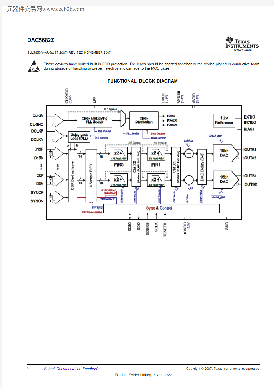
The DAC5682Z is a dual-channel 16-bit 1.0 GSPS digital-to-analog converter (DAC) with wideband LVDS data input, integrated 2x/4x interpolation filters, on-board clock multiplier and internal voltage reference. The DAC5682Z offers superior linearity, noise, crosstalk and PLL phase noise performance. The DAC5682Z integrates a wideband LVDS port with on-chip termination. Full-rate input data can be transferred to a single DAC channel, or half-rate and 1/4-rate input data can be interpolated by on-board 2x or 4x FIR filters. Each interpolation FIR is configurable in either Low-Pass or High-Pass mode, allowing selection of a higher order output spectral image. An on-chip delay lock loop (DLL) simplifies LVDS interfacing by providing skew control for the LVDS input data clock. The DAC5682Z allows both complex or real output. An optional Fs/4 coarse mixer in complex mode provides coarse frequency upconversion and the dual DAC output produces a complex Hilbert Transform pair. An external RF quadrature modulator then performs the final single sideband up-conversion. The DAC5682Z is characterized for operation over the industrial temperature range of –40°C to 85°C and is available in a 64-pin QFN package. Other single-channel members of the family include the interpolating DAC5681Z and non-interpolating DAC5681.
? ? ?
? ? ? ? ? ? ? ? ?
APPLICATIONS
Cellular Base Stations Broadband Wireless Access (BWA) WiMAX 802.16 Fixed Wireless Backhaul Cable Modem Termination System (CMTS)
ORDERING INFORMATION
TA –40°C to 85°C (1) (2) (3) ORDER CODE DAC5682ZIRGCT DAC5682ZIRGCR PACKAGE DRAWING/TYPE (1) (2) (3) RGC / 64QFN Quad Flatpack No-Lead TRANSPORT MEDIA Small Tape and Reel Large Tape and Reel QUANTITY 250 2000
Thermal Pad Size: 7,4 mm × 7,4 mm MSL Peak Temperature: Level-3-260C-168 HR For the most current package and ordering information, see the Package Option Addendum at the end of this document, or see the TI website at https://www.360docs.net/doc/c31152878.html,.
1
Please be aware that an important notice concerning availability, standard warranty, and use in critical applications of Texas Instruments semiconductor products and disclaimers thereto appears at the end of this data sheet.
PRODUCTION DATA information is current as of publication date. Products conform to specifications per the terms of the Texas Instruments standard warranty. Production processing does not necessarily include testing of all parameters.
Copyright ? 2007, Texas Instruments Incorporated
元器件交易网https://www.360docs.net/doc/c31152878.html,
DAC5682Z
SLLS853A – AUGUST 2007 – REVISED NOVEMBER 2007
https://www.360docs.net/doc/c31152878.html,
These devices have limited built-in ESD protection. The leads should be shorted together or the device placed in conductive foam during storage or handling to prevent electrostatic damage to the MOS gates.
FUNCTIONAL BLOCK DIAGRAM
CLKVDD DVDD VFUSE AVDD
(1.8V)
(1.8V)
(1.8V)
PLL Bypass
CLKIN CLKINC DCLKP DCLKN
A
Clock Multiplying PLL 2x-32x
PLL Control
Clock Distribution
FDAC FDAC/2 FDAC/4
(3.3V)
LPF
1.2V Reference
DACA_gain A-Offset 13 4
EXTIO EXTLO BIASJ
Delay Lock Loop (DLL)
B
PLL Enable
Sync Disable Mode Control
DLL Control (x2 Bypass)
[Modes = LP, HP, Fs/8, -Fs/8]
(x1 Bypass)
[Modes = LP, HP, Fs/4, -Fs/4]
D15P
100
D15N
DDR De-interleave
16
16
DAC Delay (0-3)
x2
47t 76dB HBF
x2
47t 76dB HBF
16bit DAC
IOUTA1 IOUTA2
CMIX0
D0P
100
8 Sample FIFO
FIR0 x2
47t 76dB HBF
FIR0 Enable
FIR1 x2
47t 76dB HBF
FIR1 Enable
CMIX1
D0N SYNCP
100
16
16
16bit DAC
4 DACB_gain
IOUTB1 IOUTB2
SYNCN
TXEnable=’1' SW_Sync FIFO Sync Disable
Sync & Control
(3.3V)
Delay Value
CM0 Mode
CM1 Mode
B-Offset
SYNC=’0->1' (transition)
2
2
13
2
SDENB
2
Submit Documentation Feedback Product Folder Link(s): DAC5682Z
RESETB
IOVDD
SDIO
SCLK
Copyright ? 2007, Texas Instruments Incorporated
GND
SDO
元器件交易网https://www.360docs.net/doc/c31152878.html,
DAC5682Z
https://www.360docs.net/doc/c31152878.html,
SLLS853A – AUGUST 2007 – REVISED NOVEMBER 2007
DAC5682Z RGC PACKAGE (TOP VIEW)
IOUTB1
IOUTB2
IOUTA1 AVDD
IOUTA2
AVDD EXTLO
EXTIO
53
50
64
63
62
61
60
59
58
57
56
55
52
54
51
49
RESETB
DVDD
DVDD
BIASJ
AVDD
LPF
AVDD
AVDD
CLKVDD CLKIN CLKINC GND SYNCP SYNCN D15P D15N IOVDD DVDD D14P D14N D13P D13N D12P D12N
1 2 3 4 5 6 7 8 9 10 11 12 13 14 15 16
48 47 46 45 44 43 42 41
SDENB SCLK SDIO SDO VFUSE D0N D0P D1N D1P DVDD D2N D2P D3N D3P D4N D4P
DAC5682Z
40 39 38 37 36 35 34 33
31
28
17
18
20
21
29
23
24
25
26
D11N
27
22
DCLKN
D7N
D10N
D9N
D8N
D6N
30
19
D11P
D10P
TERMINAL FUNCTIONS
TERMINAL NAME AVDD BIASJ CLKIN CLKINC CLKVDD NO. 51, 54, 55, 59, 62 57 2 3 1 7, 11, 13, 15, 17, 19, 21, 23, 27, 29, 31, 33, 35, 37, 40, 42 I/O I O I I I Analog supply voltage. (3.3V) Full-scale output current bias. For full-scale output current, connect a 960 ? resistor to GND. Positive external clock input with a self-bias of approximately CLKVDD/2. With the clock multiplier PLL enabled, CLKIN provides lower frequency reference clock. If the PLL is disabled, CLKIN directly provides clock for DAC up to 1GHz. Complementary external clock input. (See the CLKIN description) Internal clock buffer supply voltage. (1.8 V) LVDS positive input data bits 0 through 15. Each positive/negative LVDS pair has an internal 100 ? termination resistor. Order of bus can be reversed via rev_bus bit in CONFIG5 register. Data format relative to DCLKP/N clock is Double Data Rate (DDR) with two data samples input per DCLKP/N clock. In dual-channel mode, data for the A-channel is input while DCLKP is high. D15P is most significant data bit (MSB) – pin 7 D0P is least significant data bit (LSB) – pin 42 DESCRIPTION
D[15..0]P
I
DCLKP
Copyright ? 2007, Texas Instruments Incorporated
Submit Documentation Feedback Product Folder Link(s): DAC5682Z
D5N
D7P
D9P
D8P
D5P
D6P
32
3
元器件交易网https://www.360docs.net/doc/c31152878.html,
DAC5682Z
SLLS853A – AUGUST 2007 – REVISED NOVEMBER 2007
https://www.360docs.net/doc/c31152878.html,
TERMINAL FUNCTIONS (continued)
TERMINAL NAME NO. 8, 12, 14, 16, 18, 20, 22, 24, 28, 30, 32, 34, 36, 38, 41, 43 I/O DESCRIPTION LVDS negative input data bits 0 through 15. (See D[15:0]P description above) I D15N is most significant data bit (MSB) – pin 8 D0N is least significant data bit (LSB) – pin 43
D[15..0]N
DCLKP
25
I
LVDS positive input clock. Unlike the other LVDS inputs, the DCLKP/N pair is self-biased to approximately DVDD/2 and does not have an internal termination resistor in order to optimize operation of the DLL circuit. See the “DLL Operation” section. For proper external termination, connect a 100 ? resistor across LVDS clock source lines followed by series 0.01 μF capacitors connected to each of DCLKP and DCLKN pins (see Figure 26). For best performance, the resistor and capacitors should be placed as close as possible to these pins. LVDS negative input clock. (See the DCLKP description) Digital supply voltage. (1.8 V)
DCLKN DVDD EXTIO EXTLO GND
26 10, 39, 50, 63 56 58 4, Thermal Pad 52
I I
Used as external reference input when internal reference is disabled (i.e., EXTLO connected to AVDD). I/O Used as 1.2V internal reference output when EXTLO = GND, requires a 0.1 μF decoupling capacitor to AGND when used as reference output. O I Internal reference ground. Connect to AVDD to disable the internal reference. Pin 4 and the Thermal Pad located on the bottom of the QFN package is ground for AVDD, DVDD and IOVDD supplies. A-Channel DAC current output. An offset binary data pattern of 0x0000 at the DAC input results in a full scale current sink and the least positive voltage on the IOUTA1 pin. Similarly, a 0xFFFF data input results in a 0 mA current sink and the most positive voltage on the IOUTA1 pin. In single DAC mode, outputs appear on the IOUTA1/A2 pair only. A-Channel DAC complementary current output. The IOUTA2 has the opposite behavior of the IOUTA1 described above. An input data value of 0x0000 results in a 0mA sink and the most positive voltage on the IOUTA2 pin. B-Channel DAC current output. See the IOUTA1 description above. B-Channel DAC complementary current output. See the IOUTA2 description above. Digital I/O supply voltage (3.3V) for pins RESETB, SCLK, SDENB, SDIO, SDO. PLL loop filter connection. If not using the clock multiplying PLL, the LPF pin may be left open. Set both PLL_bypass and PLL_sleep control bits for reduced power dissipation. Resets the chip when low. Internal pull-up. Serial interface clock. Internal pull-down. Active low serial data enable, always an input to the DAC5682Z. Internal pull-up. Serial interface data, uni-directional data output, if SDIO is an input. SDO is 3-stated when the 3 pin interface mode is selected (register 0x08 bit 1). Internal pull-down. LVDS SYNC positive input data. The SYNCP/N LVDS pair has an internal 100 ? termination resistor. By default, the SYNCP/N input must be logic ‘1’ to enable a DAC analog output. See the LVDS SYNCP/N Operation paragraph for a detailed description. LVDS SYNC negative input data. Digital supply voltage. (1.8V) Connect to DVDD pins for normal operation. This supply pin is also used for factory fuse programming.
IOUTA1
O
IOUTA2 IOUTB1 IOUTB2 IOVDD LPF RESETB SCLK SDENB SDIO SDO SYNCP SYNCN VFUSE
53 61 60 9 64 49 47 48 46 45 5 6 44
O O O I I I I I
I/O Serial interface data, bi-directional. Default setting sets SDIO as an input. Internal pull-down. O I I I
4
Submit Documentation Feedback Product Folder Link(s): DAC5682Z
Copyright ? 2007, Texas Instruments Incorporated
元器件交易网https://www.360docs.net/doc/c31152878.html,
DAC5682Z
https://www.360docs.net/doc/c31152878.html,
SLLS853A – AUGUST 2007 – REVISED NOVEMBER 2007
ABSOLUTE MAXIMUM RATINGS
over operating free-air temperature range (unless otherwise noted)
DVDD Supply voltage range
(2) (1)
VALUE –0.5 to 2.3 –0.5 to 2.3 –0.5 to 4 –0.5 to 4 –0.5 to 0.5 –2 to 2.6 –0.5 to 0.5 –0.5 to 0.5
(2)
UNIT V V V V V V V V V V V V V V mA mA °C °C
CLKVDD (2) AVDD (2) IOVDD
(2)
Voltage between GND, and CLKGND AVDD to DVDD CLKVDD to DVDD IOVDD to AVDD D[15..0]P ,D[15..0]N, SYNCP, SYNCN Supply voltage range DCLKP, DCLKN (2) CLKIN, CLKINC
(2) (2)
–0.5 to DVDD + 0.5 –0.3 to 2.1 –0.5 to CLKVDD + 0.5 –0.5 to IOVDD + 0.5 –0.5 to AVDD + 0.5 –0.5 to AVDD + 0.5 20 –30 –40 To 85 –65 To 150
SDO, SDIO, SCLK, SDENB, RESETB IOUTA1/B1, IOUTA2/B2 Peak input current (any input) Peak total input current (all inputs) Operating free-air temperature range, TA: DAC5682ZI Storage temperature range (1) (2)
(2) (2)
LPF, EXTIO, EXTLO, BIASJ
Stresses beyond those listed under absolute maximum ratings may cause permanent damage to the device. These are stress ratings only, and functional operation of these or any other conditions beyond those indicated under recommended operating conditions is not implied. Exposure to absolute-maximum-rated conditions for extended periods may affect device reliability. Measured with respect to GND.
THERMAL CHARACTERISTICS
over operating free-air temperature range (unless otherwise noted)
THERMAL CONDUCTIVITY TJ θJA θJC θJP (1) Maximum junction temperature
(1)
64ld QFN 125 20 16 7 0.2
UNIT °C °C/W °C/W °C/W
Theta junction-to-ambient (still air) Theta junction-to-ambient (150 lfm) Theta junction-to-case Theta junction-to-pad
Air flow or heat sinking reduces θJA and may be required for sustained operation at 85° under maximum operating conditions.
Copyright ? 2007, Texas Instruments Incorporated
Submit Documentation Feedback Product Folder Link(s): DAC5682Z
5
元器件交易网https://www.360docs.net/doc/c31152878.html,
DAC5682Z
SLLS853A – AUGUST 2007 – REVISED NOVEMBER 2007
https://www.360docs.net/doc/c31152878.html,
ELECTRICAL CHARACTERISTICS — DC SPECIFICATION
over operating free-air temperature range , AVDD = 3.3 V, CLKVDD = 1.8 V, IOVDD = 3.3 V, DVDD = 1.8 V, IoutFS = 20 mA (unless otherwise noted)
PARAMETER Resolution DC ACCURACY INL DNL
(1)
TEST CONDITIONS
MIN 16
TYP
MAX
UNIT Bits
Integral nonlinearity Differential nonlinearity Course gain linearity Offset error Gain error Gain error Gain mismatch Minimum full scale output current (2) Maximum full scale output current (2) Output Compliance range (3) Output resistance Output capacitance
1 LSB = IOUTFS/216
±4 ±2 ±0.04
LSB
ANALOG OUTPUT LSB %FSR %FSR %FSR 2 2 20 IOUTFS = 20 mA AVDD –0.5V 300 5 1.14
(4)
Mid code offset Without internal reference With internal reference With internal reference, dual DAC, SSB mode –2
0.01 1 0.7
%FSR mA
AVDD + 0.5V
V k? pF
REFERENCE OUTPUT Vref Reference voltage Reference output current REFERENCE INPUT VEXTIO Input voltage range Input resistance Small signal bandwidth Input capacitance TEMPERATURE COEFFICIENTS Offset drift Gain drift Reference voltage drift POWER SUPPLY Analog supply voltage, AVDD Digital supply voltage, DVDD Clock supply voltage, CLKVDD I/O supply voltage, IOVDD I(AVDD) I(DVDD) I(CLKVDD) I(IOVDD) Analog supply current Digital supply current Clock supply current IO supply current Mode 4 (below) 3.0 1.71 1.71 3.0 3.3 1.8 1.8 3.3 133 455 45 12 3.6 2.15 2.15 3.6 V V V V mA mA mA mA Without internal reference With internal reference ±1 ±15 ±30 ±8 ppm of FSR/°C ppm of FSR/°C ppm/°C CONFIG6: BiasLPF_A and BiasLPF = 1 CONFIG6: BiasLPF_A and BiasLPF = 0 0.1 1 95 472 100 1.25 V M? kHz pF 1.2 100 1.26 V nA
(1) (2) (3) (4) 6
Measured differential across IOUTA1 and IOUTA2 or IOUTB1 and IOUTB2 with 25 ? each to AVDD. Nominal full-scale current, IoutFS, equals 16 × IBIAS current. The lower limit of the output compliance is determined by the CMOS process. Exceeding this limit may result in transistor breakdown, resulting in reduced reliability of the DAC5682Z device. The upper limit of the output compliance is determined by the load resistors and full-scale output current. Exceeding the upper limit adversely affects distortion performance and integral nonlinearity. Use an external buffer amplifier with high impedance input to drive any external load. Submit Documentation Feedback Product Folder Link(s): DAC5682Z
Copyright ? 2007, Texas Instruments Incorporated
元器件交易网https://www.360docs.net/doc/c31152878.html,
DAC5682Z
https://www.360docs.net/doc/c31152878.html,
SLLS853A – AUGUST 2007 – REVISED NOVEMBER 2007
ELECTRICAL CHARACTERISTICS — DC SPECIFICATION (continued)
over operating free-air temperature range , AVDD = 3.3 V, CLKVDD = 1.8 V, IOVDD = 3.3 V, DVDD = 1.8 V, IoutFS = 20 mA (unless otherwise noted)
PARAMETER I(AVDD) I(DVDD) I(CLKVDD) I(IOVDD) Sleep mode, AVDD supply current Sleep mode, DVDD supply current Sleep mode, CLKVDD supply current Sleep mode, IOVDD supply current AVDD + IOVDD current, 3.3V DVDD + CLKVDD current, 1.8V Power Dissipation AVDD + IOVDD current, 3.3V DVDD + CLKVDD current, 1.8V Power Dissipation AVDD + IOVDD current, 3.3V DVDD + CLKVDD current, 1.8V P Power Dissipation AVDD + IOVDD current, 3.3V DVDD + CLKVDD current, 1.8V Power Dissipation AVDD + IOVDD current, 3.3V DVDD + CLKVDD current, 1.8V Power Dissipation AVDD + IOVDD current, 3.3V DVDD + CLKVDD current, 1.8V Power Dissipation PSSR T Power supply rejection ratio Operating range –2 –40 Mode 2: 2X2, PLL = ON (8X), CLKIN = 122.88 MHz FDAC = 983.04MHz, IF = 184.32 MHz DACA and DACB ON, 4 carrier WCDMA Mode 3: 2X4, CMIX0 = Fs/4, PLL = OFF, CLKIN = 983.04 MHz FDAC = 983.04MHz, IF = 215.04 MHz DACA and DACB ON, 4 carrier WCDMA Mode 4: 2X4, CMIX0 = Fs/4, PLL = ON (8X), CLKIN = 122.88 MHz FDAC = 983.04MHz, IF = 215.04 MHz DACA and DACB ON, 4 carrier WCDMA Mode 5: 2X2, CMIX0 = Fs/4, PLL = OFF, CLKIN = 983.04 MHz FDAC = 983.04MHz, Digital Logic Disabled DACA and DACB SLEEP, Static Data Pattern Mode 6: 2X4, PLL = OFF, CLKIN = OFF FDAC = OFF, Digital Logic Disabled DACA and DACB = SLEEP, Static Data Pattern Mode 1: 2X2, PLL = OFF, CLKIN = 983.04 MHz FDAC = 983.04MHz, IF = 184.32 MHz DACA and DACB ON, 4 carrier WCDMA Mode 6 (below) TEST CONDITIONS MIN TYP 1.0 1.5 2.5 2.0 135 450 1255 145 485 1350 135 480 1310 145 505 1400 5 185 350 3.0 4.0 17.0 30.0 85 1600 MAX UNIT mA mA mA mA mA mA mW mA mA mW mA mA mW mA mA mW mA mA mW mA mA mW °C 0.2 %FSR/V
Copyright ? 2007, Texas Instruments Incorporated
Submit Documentation Feedback Product Folder Link(s): DAC5682Z
7
元器件交易网https://www.360docs.net/doc/c31152878.html,
DAC5682Z
SLLS853A – AUGUST 2007 – REVISED NOVEMBER 2007
https://www.360docs.net/doc/c31152878.html,
ELECTRICAL CHARACTERISTICS — AC SPECIFICATION (1)
Over recommended operating free-air temperature range, AVDD, IOVDD = 3.3 V, CLKVDD, DVDD = 1.8 V, IOUTFS = 20 mA, 4:1 transformer output termination, 50? doubly terminated load (unless otherwise noted)
PARAMETER ANALOG OUTPUT fCLK ts(DAC) tpd tr(IOUT) tf(IOUT) Maximum output update rate Output settling time to 0.1% Output propagation delay Output rise time 10% to 90% Output fall time 90% to 10% 1X1, PLL off, CLKIN = 500 MHz, DACA on, IF = 5.1 MHz, First Nyquist Zone < fDATA/2 SFDR Spurious free dynamic range 2X2, PLL off, CLKIN = 1000 MHz, DACA and DACB on, IF = 5.1 MHz, First Nyquist Zone < fDATA/2 2X2, PLL off, CLKIN = 1000 MHz, DACA and DACB on, IF = 20.1 MHz, First Nyquist Zone < fDATA/2 2X2, PLL off, CLKIN = 500 MHZ, DACA and DACB on, Single tone, 0 dBFS, IF = 20.1 MHz 2X2, PLL off, CLKIN = 1000 MHZ, DACA and DACB on, Single tone, 0 dBFS, IF = 20.1 MHz 2X2, PLL off, CLKIN = 1000 MHZ, DACA and DACB on, Single tone, 0 dBFS, IF = 70.1 MHz 2X4, PLL off, CLKIN = 1000 MHZ, DACA and DACB on, Single tone, 0 dBFS, IF = 180 MHz 2X2 CMIX, PLL off, CLKIN = 1000 MHZ, DACA and DACB on, Single tone, 0 dBFS, IF = 300.2 MHz 2X2, PLL off, CLKIN = 1000 MHZ, DACA and DACB on, Four tone, each -12 dBFS, IF = 24.7, 24.9, 25.1 and 25.3 MHz 2X2, PLL off, CLKIN = 1000 MHZ, DACA and DACB on, IF = 20.1 and 21.1 MHz IMD3 Third-order two-tone intermodulation (each tone at –6 dBFS) 2X2, PLL off, CLKIN = 1000 MHZ, DACA and DACB on, IF = 70.1 and 71.1 MHz 2X2 CMIX, PLL off, CLKIN = 1000 MHZ, DACA and DACB on, IF = 150.1 and 151.1 MHz IMD Four-tone intermodulation (each tone at –12 dBFS) 2X2 CMIX, PLL off, CLKIN = 1000 MHz, DACA and DACB on, fOUT = 298.4, 299.2, 300.8 and 301.6 MHz Single carrier, baseband, 2X2, PLL off, CLKIN = 983.04 MHz, DACA and DACB on (3)
(2)
TEST CONDITIONS
MIN
TYP MAX
UNIT
1000 Transition: Code 0x0000 to 0xFFFF 10.4 3 2 2
MSPS ns ns ns ns
AC PERFORMANCE 81 80 77 73 69 63 dBc 60 60 73 81 72 64 64 80 83 73 dBc 66 63 93 dBc 85 dBc dBc dBc
SNR
Signal-to-noise ratio
ACLR
Adjacent channel leakage ratio
Single carrier, IF = 180 MHz, 2X2, PLL off, CLKIN = 983.04 MHz, DACA and DACB on Four carrier, IF = 180 MHz, 2X2 CMIX, PLL off, CLKIN = 983.04 MHz, DACA and DACB on Four carrier, IF = 275 MHz, 2X2 CMIX, PLL off, CLKIN = 983.04 MHz, DACA and DACB on
Noise floor
(4)
50-MHz offset, 1-MHz BW, Single Carrier, baseband, 2X2, PLL off, CLKIN = 983.04 50-MHz offset, 1-MHz BW, Four Carrier, baseband, 2X2, PLL off, CLKIN = 983.04.
(1) (2) (3) (4)
Measured single-ended into 50 ? load. W-CDMA with 3.84 MHz BW, 5-MHz spacing, centered at IF. TESTMODEL 1, 10 ms Valid over 25°C to 85°C Carrier power measured in 3.84 MHz BW.
8
Submit Documentation Feedback Product Folder Link(s): DAC5682Z
Copyright ? 2007, Texas Instruments Incorporated
元器件交易网https://www.360docs.net/doc/c31152878.html,
DAC5682Z
https://www.360docs.net/doc/c31152878.html,
SLLS853A – AUGUST 2007 – REVISED NOVEMBER 2007
ELECTRICAL CHARACTERISTICS (DIGITAL SPECIFICATIONS)
over recommended operating free-air temperature range, AVDD, IOVDD = 3.3V, CLKVDD, DVDD = 1.8V.
PARAMETER Positive-going differential input voltage threshold Negative-going differential input voltage threshold Input Common Mode Input Common Mode LVDS Input capacitance DCLK to Data DCLKP/N: 0 to 125MHz (see Figure 33) CONFIG5 DLL_bypass = 1, CONFIG10 = '00000000' DCLKP/N = 150MHz CONFIG5 DLL_bypass = 0, DCLKP/N = 200MHz CONFIG5 DLL_bypass = 0 DCLKP/N = 250MHz CONFIG5 DLL_bypass = 0 DCLK to Data Skew (1) [Please contact factory for recommended DLL settings] DCLKP/N = 300MHz CONFIG5 DLL_bypass = 0 DCLKP/N = 350 MHz CONFIG5 DLL_bypass = 0 DCLKP/N = 400 MHz CONFIG5 DLL_bypass = 0 Refer to supported data rate [fDATA ] DCLKP/N = 450 MHz CONFIG5 DLL_bypass = 0 Refer to supported data rate [fDATA ] DCLKP/N = 500 MHz, T = 25 °C to 85 °C CONFIG5 DLL_bypass = 0 Refer to supported data rate [fDATA ] DLL Enabled, T = 25 °C to 85 °C DDR format, DCLKP frequency: 125 to 500 MHz fDATA Input data rate supported DLL Enabled, T = –40 °C DDR format, DCLK frequency: 125 to 375 MHz DLL Disabled, T = –40 °C to 85 °C DDR format, DCLKP frequency: <125 MHz CMOS INTERFACE: SDO, SDIO, SCLK, SDENB, RESETB VIH VIL IIH IIL CI (1) High-level input voltage Low-level input voltage High-level input current Low-level input current CMOS Input capacitance Positive skew: Clock ahead of data. Negative skew: Data ahead of clock. Submit Documentation Feedback Product Folder Link(s): DAC5682Z 9 2 0 –40 –40 5 3 0 0.8 40 40 V V μA μA pF Setup_min Hold_min Positive Negative Positive Negative Positive Negative Positive Negative Positive Negative Positive Negative Positive Negative Positive Negative 250 250 SYNCP/N, D[15:0]P and D[15:0]N only DCLKP/N only 100 TEST CONDITIONS MIN TYP 175 mV –175 mV 1.2 DVDD/ 2 110 2 1100 –600 1000 –1800 800 –1300 600 –1000 450 –800 400 –700 300 –600 300 –500 350 –300 1000 750 250 MSPS ps 120 V V ? pF MAX UNIT LVDS INTERFACE: D[15:0]P, D[15:0]N, SYNCP/N, DCLKP/N VITH+
VITH– VCOM1 VCOM2 ZT CL tS, tH
Internal termination SYNCP/N, D[15:0]P and D[15:0]N only
tSKEW(A), tSKEW(B)
Copyright ? 2007, Texas Instruments Incorporated
元器件交易网https://www.360docs.net/doc/c31152878.html,
DAC5682Z
SLLS853A – AUGUST 2007 – REVISED NOVEMBER 2007
https://www.360docs.net/doc/c31152878.html,
ELECTRICAL CHARACTERISTICS (DIGITAL SPECIFICATIONS) (continued)
over recommended operating free-air temperature range, AVDD, IOVDD = 3.3V, CLKVDD, DVDD = 1.8V.
PARAMETER Iload = –100 μA VOH SDO, SDIO Iload = –2mA Iload = 100 μA VOL SDO, SDIO Setup time, SDENB to rising edge of SCLK Setup time, SDIO valid to rising edge of SCLK Hold time, SDIO valid to rising edge of SCLK Period of SCLK High time of SCLK Low time of SCLK Data output delay after falling edge of SCLK Minimum RESETB pulse width Duty cycle Differential voltage CLKIN/CLKINC input common mode PHASE LOCKED LOOP DAC output at 600 kHz offset, 100 MHz, 0-dBFS tone, 2X4, fDATA = 250 MSPS, CLKIN/C = 250 MHz, PLL_m = '00111', PLL_n = '001', VCO_div2 = 0, PLL_range = '1111', PLL_gain = '00' DAC output at 6 MHz offset, 100 MHz, 0-dBFS tone, 2X4, fDATA = 250 MSPS, CLKIN/C = 250 MHz, PLL_m = '00111', PLL_n = '001', VCO_div2 = 0, PLL_range = '1111', PLL_gain = '00' 0.5 Iload = 2 mA 20 0.22 x IOVDD TEST CONDITIONS MIN TYP IOVDD – 0.2 0.8 x IOVDD 0.2 MAX UNIT V V V V ns
ts(SDENB)
ts(SDIO)
10
ns
th(SDIO) t(SCLK) t(SCLKH) t(SCLK) td(Data) tRESET
5 100 40 40 10 25
ns ns ns ns ns ns
CLOCK INPUT (CLKIN/CLKINC) 50% 1 CLKVD D/2 V V
–125 dBc/ Hz –146
Phase noise
10
Submit Documentation Feedback Product Folder Link(s): DAC5682Z
Copyright ? 2007, Texas Instruments Incorporated
元器件交易网https://www.360docs.net/doc/c31152878.html,
DAC5682Z
https://www.360docs.net/doc/c31152878.html,
SLLS853A – AUGUST 2007 – REVISED NOVEMBER 2007
ELECTRICAL CHARACTERISTICS (DIGITAL SPECIFICATIONS) (continued)
over recommended operating free-air temperature range, AVDD, IOVDD = 3.3V, CLKVDD, DVDD = 1.8V.
PARAMETER TEST CONDITIONS PLL_gain = '00', PLL_range = '0000' (0) PLL_gain = '01', PLL_range = '0001' (1) PLL_gain = '01', PLL_range = '0010' (2) PLL_gain = '01', PLL_range = '0011' (3) PLL_gain = '01', PLL_range = '0100' (4) PLL_gain = '10', PLL_range = '0101' (5) PLL_gain = '10', PLL_range = '0110' (6) PLL_gain = '10', PLL_range = '0111' (7) PLL_gain = '10', PLL_range = '1000' (8) PLL_gain = '10', PLL_range = '1001' (9) PLL_gain = '11', PLL_range = '1010' (A) PLL_gain = '11', PLL_range = '1011' (B) PLL_gain = '11', PLL_range = '1100' (C) PLL_gain = '11', PLL_range = '1101' (D) PLL_gain = '11', PLL_range = '1110' (E) PLL_gain = '11', PLL_range = '1111' (F) PFD Maximum Frequency MIN 160 220 290 300 400 260 480 240 560 210 620 270 690 250 PLL/VCO Operating Frequency, Typical VCO Gain 740 240 790 220 840 210 880 250 920 230 960 220 1000 210 1030 200 1060 190 160 1090 1070 1040 1020 990 940 880 850 820 780 740 620 570 520 460 TYP MAX 290 UNIT MHz MHz/V MHz MHz/V MHz MHz/V MHz MHz/V MHz MHz/V MHz MHz/V MHz MHz/V MHz MHz/V MHz MHz/V MHz MHz/V MHz MHz/V MHz MHz/V MHz MHz/V MHz MHz/V MHz MHz/V MHz MHz/V MHz
Copyright ? 2007, Texas Instruments Incorporated
Submit Documentation Feedback Product Folder Link(s): DAC5682Z
11
元器件交易网https://www.360docs.net/doc/c31152878.html,
DAC5682Z
SLLS853A – AUGUST 2007 – REVISED NOVEMBER 2007
https://www.360docs.net/doc/c31152878.html,
TYPICAL CHARACTERISTICS
10 8 6 4
DNL - LSB
10 8 6 4 2 0 -2 -4 -6 -8
INL - LSB
2 0 -2 -4 -6 -8 -10 0 10000 20000 30000 40000 50000 60000 Code
Figure 1. Integral Nonlinearity
-10 0 10000 20000 30000 40000 50000 60000 Code Figure 2. Differential Nonlinearity
10 0 -10 -20
Power - dBm
10
Fdata = 250 MSPS, FIN = 20 MHz Complex, IF = 20 MHz, x4 Interpolation PLL Off
Power - dBm
0 -10 -20 -30 -40 -50 -60 -70 -80 -90
-30 -40 -50 -60 -70 -80 -90 0 50 100 150 200 250 300 350 400 450 500 f - Frequency - MHz
Figure 3. Single-Tone Spectral Plot
Fdata = 250 MSPS, FIN = 20 MHz Complex, IF = 270 MHz, x4 Interpolation CMIX FS/4 PLL Off
0
50 100 150 200 250 300 350 400 450 500 f - Frequency - MHz
Figure 4. Single-Tone Spectral Plot
12
Submit Documentation Feedback Product Folder Link(s): DAC5682Z
Copyright ? 2007, Texas Instruments Incorporated
元器件交易网https://www.360docs.net/doc/c31152878.html,
DAC5682Z
https://www.360docs.net/doc/c31152878.html,
SLLS853A – AUGUST 2007 – REVISED NOVEMBER 2007
TYPICAL CHARACTERISTICS (continued)
10
SFDR - Spurious Free Dynamic Range - dBc
95 Fdata = 250 MSPS, FIN = -80 MHz Complex, (-80+250=170) IF = 170 MHz, CMIX, FS/4 x4 Interpolation PLL Off Fdata = 250 MSPS, x4 Interpolation, PLL Off
0 -10 -20
Power - dBm
90
85 -6 dBFS -12 dBFS 80
-30 -40 -50 -60 -70 -80 0
75
70 0 dBFS 65 60 0
50
100 150 200 250 300 350 400 450 500 f - Frequency - MHz
Figure 5. Single-Tone Spectral Plot
10 20 30 40 IF - Intermediate Frequency - MHz
Figure 6. In-Band SFDR vs IF
50
90
90
Fdata = 250 MSPS, x4 Interpolation, PLL Off
SFDR - Spurious-Free Dynamic Range - dBc
85 80 75 70 65 60 55
85 80
IMD - dBc
Fdata = 250 MSPS, x4 Interpolation, PLL Off
75 70 65 60
50 45 40 0 50 100 150 200 250 300 350 400 450 500 IF - Intermediate Frequency - MHz
55 50 0
40
80 120 160 200 240 280 IF - Intermediate Frequency - MHz
320
Figure 7. Out-Of-Band SFDR vs IF
Figure 8. Two Tone IMD vs Output Frequency
Copyright ? 2007, Texas Instruments Incorporated
Submit Documentation Feedback Product Folder Link(s): DAC5682Z
13
元器件交易网https://www.360docs.net/doc/c31152878.html,
DAC5682Z
SLLS853A – AUGUST 2007 – REVISED NOVEMBER 2007
https://www.360docs.net/doc/c31152878.html,
TYPICAL CHARACTERISTICS (continued)
85 80 75 -30 89.5 and 90.5 MHz (CMIX Off) 0 -10 F = 40 ± 0.5 MHz Real, IN -20 x2 Interpolation
PLL Off IF = 40 MHz, Fdata = 500 MSPS,
Power - dBm
70
-40 -50 -60 -70 -80 -90 -100 35
IMD - dBc
65 Shift to 340 MHz (FS/8 On) 60 55 50 45 -30 Shift to 215 MHz (FS/4 On) Fdata = 250 MSPS Fin = 90 MHz ±0.5 MHz Complex x4 Interpolation, PLL Off Three modes: CMIX, FS/8, and FS/4 -25 -20 -15 -10 -5 Amplitude - dBFS Figure 9. Two Tone IMD vs Amplitude 0
36
37
38
39 40 41 42 f - Frequency - MHz
43
44
45
Figure 10. Two-Tone IMD Spectral Plot
85 Fdata = 491.52 MSPS, FIN = IF 80
10
Fdata = 500 MSPS,
0 FIN = 0 ± 0.5 MHz,
IF = 250 MHz (Fs/4) -10 x2 Interpolation PLL Off
-20
Power - dBm
-30 -40 -50 -60
ACLR - dBc
PLL Off 75 PLL On
70
-70 -80 -90 248.5 249.0 249.5 250.0 250.5 251.0 251.5 252.0 252.5 f - Frequency - MHz
65 0 61.44 122.88 184.32 f - Frequency - MHz 245.76
Figure 11. Two-Tone IMD Spectral Plot
Figure 12. Single Carrier W-CDMA Test Model 1
14
Submit Documentation Feedback Product Folder Link(s): DAC5682Z
Copyright ? 2007, Texas Instruments Incorporated
元器件交易网https://www.360docs.net/doc/c31152878.html,
DAC5682Z
https://www.360docs.net/doc/c31152878.html,
SLLS853A – AUGUST 2007 – REVISED NOVEMBER 2007
TYPICAL CHARACTERISTICS (continued)
-20 -30 -40 -50
Power - dBm
Carrier Power: -7.60 dBm, ACLR (5 MHz): 80.66 dB, ACLR (10 MHz): 82.61 dB, Fdata = 245.76 MSPS, IF = 61.44 MHz, x4 Interpolation PLL Off
-20 -30 ACLR (10 MHz): 82.45 dB,
Fdata = 245.76 MSPS, Carrier Power: -7.60 dBm, ACLR (5 MHz): 77.49 dB,
-40 IF = 61.44 MHz,
x4 Interpolation
-50 PLL On
-60 -70 -80 -90 -100 -110 -120 48.9
Power - dBm
-60 -70 -80 -90 -100 -110 -120 48.9
53.9
58.9 63.9 f - Frequency - MHz
68.9
73.9
53.9
58.9 63.9 f - Frequency - MHz
68.9
73.9
Figure 13. Single Carrier W-CDMA Test Model 1
Figure 14. Single Carrier W-CDMA Test Model 1
-20
Carrier Power: -8.66 dBm, ACLR (5 MHz): 68.61 dB,
-20 -30 -40 -50
Power - dBm
Carrier Power: -8.66 dBm, ACLR (5 MHz): 73.19 dB, ACLR (10 MHz): 80.07 dB, Fdata = 491.52 MSPS, IF = 184.32 MHz, x2 Interpolation PLL Off
-30 ACLR (10 MHz): 75.91 dB,
Fdata = 491.52 MSPS,
-40 IF = 184.32 MHz,
x2 Interpolation PLL On
-50
-60 -70 -80 -90 -100 -110 -120 172
Power - dBm
-60 -70 -80 -90 -100 -110
177
182 187 f - Frequency - MHz
192
197
-120 172
177
182 187 f - Frequency - MHz
192
197
Figure 15. Single Carrier W-CDMA Test Model 1
Figure 16. Single Carrier W-CDMA Test Model 1
Copyright ? 2007, Texas Instruments Incorporated
Submit Documentation Feedback Product Folder Link(s): DAC5682Z
15
元器件交易网https://www.360docs.net/doc/c31152878.html,
DAC5682Z
SLLS853A – AUGUST 2007 – REVISED NOVEMBER 2007
https://www.360docs.net/doc/c31152878.html,
TYPICAL CHARACTERISTICS (continued)
-20 -30 -40 -50
Carrier Power: -8.99 dBm, ACLR (5 MHz): 68.22 dB, ACLR (10 MHz): 74.15 dB, Fdata = 245.76 MSPS, IF = Baseband, x4 Interpolation CMIX PLL Off
-20
Carrier Power: -8.99 dBm, ACLR (5 MHz): 64.23 dB,
-30 ACLR (10 MHz): 71.27 dB,
Fdata = 245.76 MSPS,
-40 IF = Baseband, -50
x4 Interpolation CMIX PLL On
Power - dBm
-60 -70 -80 -90 -100 -110 -120 233
Power - dBm
238 243 248 f - Frequency - MHz 253 258
-60 -70 -80 -90 -100 -110 -120 233
238
243 248 f - Frequency - MHz
253
258
Figure 17. Single Carrier W-CDMA Test Model 1 -20 Carrier Power: -11.98 dBm,
ACLR (5 MHz): 69.74 dB,
Figure 18. Single Carrier W-CDMA Test Model 1 -20 Carrier Power: -11.98 dBm,
ACLR (5 MHz): 66.16 dB,
-30 ACLR (10 MHz): 75.41 dB,
F -40 x2 Interpolation
-30 ACLR (10 MHz): 72.84 dB,
F -40 x2 Interpolation
Fdata = 491.52 MSPS, I = 184.32 MHz, PLL Off
Fdata = 491.52 MSPS, I = 184.32 MHz, PLL On
-50
-50
Power - dBm
-60 -70 -80 -90 -100 -110 -120 160 165 170 175 180 185 190 195 200 205 210 f - Frequency - MHz
Power - dBm
Figure 19. Two Carrier W-CDMA Test Model 1
-60 -70 -80 -90 -100 -110 -120 160 165 170 175 180 185 190 195 200 205 210 f - Frequency - MHz
Figure 20. Two Carrier W-CDMA Test Model 1
16
Submit Documentation Feedback Product Folder Link(s): DAC5682Z
Copyright ? 2007, Texas Instruments Incorporated
元器件交易网https://www.360docs.net/doc/c31152878.html,
DAC5682Z
https://www.360docs.net/doc/c31152878.html,
SLLS853A – AUGUST 2007 – REVISED NOVEMBER 2007
TYPICAL CHARACTERISTICS (continued)
-20 Carrier Power: -15.85 dBm, -30 -40 -50
Power - dBm
ACLR (5 MHz): 69.66 dB, ACLR (10 MHz): 70.65 dB, Fdata = 491.52 MSPS, IF = 184.32 MHz, x2 Interpolation PLL Off
-20 Carrier Power: -15.85 dBm,
ACLR (5 MHz): 65.85 dB,
-30 ACLR (10 MHz): 69.60 dB,
F -40 x2 Interpolation
Fdata = 491.52 MSPS, I = 184.32 MHz, PLL On
-50
-60 -70 -80 -90 -100 -110 -120 160 165 170 175 180 185 190 195 200 205 210 f - Frequency - MHz
Figure 21. Four Carrier W-CDMA Test Model 1 -20 Carrier Power: -15.20 dBm,
ACLR (5 MHz): 71.18 dB,
Power - dBm
-60 -70 -80 -90 -100 -110 -120 160 165 170 175 180 185 190 195 200 205 210 f - Frequency - MHz
Figure 22. Four Carrier W-CDMA Test Model 1
-20
Carrier Power: -15.20 dBm, ACLR (5 MHz): 66.53 dB, Fdata = 491.52 MSPS, I = 184.32 MHz, PLL On
-30 ACLR (10 MHz): 72.26 dB, -40 x2 Interpolation
PLL Off Fdata = 491.52 MSPS, IF = 184.32 MHz,
-30 ACLR (10 MHz): 69.68 dB,
F -40 x2 Interpolation
-50
-50
Power - dBm
-60 -70 -80 -90 -100 -110 -120 160 165 170 175 180 185 190 195 200 205 210 f - Frequency - MHz
Power - dBm
-60 -70 -80 -90 -100 -110 -120 160 165 170 175 180 185 190 195 200 205 210 f - Frequency - MHz
Figure 23. Three Carrier W-CDMA Test Model 1 with Gap
Figure 24. Three Carrier W-CDMA Test Model 1 with Gap
TEST METHODOLOGY
Typical AC specifications were characterized with the DAC5682ZEVM using the test configuration shown in Figure 25. A sinusoidal master clock frequency is generated by an HP8665B signal generator and into a splitter. One output drives an Agilent 8133A pulse generator, and the other drives the CDCM7005 clock driver. The 8133A converts the sinusoidal frequency into a square wave output clock and drives an Agilent ParBERT 81250A pattern-generator clock. On the EVM, the DAC5682Z CLKIN/C input clock is driven by an CDCM7005 clock distribution chip that is configured to simply buffer the external 8665B clock or divide it down for PLL test configurations. The DAC5682Z output is characterized with a Rohde and Schwarz FSU spectrum analyzer. For WCDMA signal characterization, it is important to use a spectrum analyzer with high IP3 and noise subtraction capability so that the spectrum analyzer does not limit the ACPR measurement. For all specifications, both DACA and DACB are measured and the lowest value used as the specification.
Copyright ? 2007, Texas Instruments Incorporated
Submit Documentation Feedback Product Folder Link(s): DAC5682Z
17
元器件交易网https://www.360docs.net/doc/c31152878.html,
DAC5682Z
SLLS853A – AUGUST 2007 – REVISED NOVEMBER 2007
https://www.360docs.net/doc/c31152878.html,
Agilent 81205A ParBERT
D15
P N
DAC5682ZEVM SMA Adapter Board DAC5682Z DAC
Stacking Interface Connector
100
3.3 V
100
3.3 V
FIFO & Demux
DAC-A
CMIX1
100
N
100
CMIX0
D0 Pattern Memory
P
3.3 V
100
3.3 V
Rohde & Schwartz FSU Spectrum Analyzer
I-FIR0
I-FIR1
Q-FIR0
SYNC
P N
Q-FIR1
3.3 V
100
DAC-B
100
DCLK
P N
100
DLL
opt. PLL
CLKIN CLKINC
3.3 V
Swap Cable For DAC-B measurements
36 each SMA-SMA cables
Loop Filter
CDCM7005
Opt. Clock Divider
Splitter
100
Optional Divider
Agilent 8133A Pulse Generator
HP8665B Synthesized Signal Generator
DAC5682ZEVM
Figure 25. DAC5682Z Test Configuration for Normal Clock Mode
DEFINITION OF SPECIFICATIONS
Adjacent Carrier Leakage Ratio (ACLR): Defined for a 3.84Mcps 3GPP W-CDMA input signal measured in a 3.84MHz bandwidth at a 5MHz offset from the carrier with a 12dB peak-to-average ratio. Analog and Digital Power Supply Rejection Ratio (APSSR, DPSSR): Defined as the percentage error in the ratio of the delta IOUT and delta supply voltage normalized with respect to the ideal IOUT current. Differential Nonlinearity (DNL): Defined as the variation in analog output associated with an ideal 1 LSB change in the digital input code. Gain Drift: Defined as the maximum change in gain, in terms of ppm of full-scale range (FSR) per °C, from the value at ambient (25°C) to values over the full operating temperature range. Gain Error: Defined as the percentage error (in FSR%) for the ratio between the measured full-scale output current and the ideal full-scale output current. Integral Nonlinearity (INL): Defined as the maximum deviation of the actual analog output from the ideal output, determined by a straight line drawn from zero scale to full scale. Intermodulation Distortion (IMD3, IMD): The two-tone IMD3 or four-tone IMD is defined as the ratio (in dBc) of the worst 3rd-order (or higher) intermodulation distortion product to either fundamental output tone. Offset Drift: Defined as the maximum change in DC offset, in terms of ppm of full-scale range (FSR) per °C, from the value at ambient (25°C) to values over the full operating temperature range. Offset Error: Defined as the percentage error (in FSR%) for the ratio of the differential output current (IOUT1–IOUT2) and the mid-scale output current. Output Compliance Range: Defined as the minimum and maximum allowable voltage at the output of the current-output DAC. Exceeding this limit may result reduced reliability of the device or adversely affecting distortion performance. Reference Voltage Drift: Defined as the maximum change of the reference voltage in ppm per degree Celsius from value at ambient (25°C) to values over the full operating temperature range. Spurious Free Dynamic Range (SFDR): Defined as the difference (in dBc) between the peak amplitude of the output signal and the peak spurious signal.
18
Submit Documentation Feedback Product Folder Link(s): DAC5682Z
Copyright ? 2007, Texas Instruments Incorporated
元器件交易网https://www.360docs.net/doc/c31152878.html,
DAC5682Z
https://www.360docs.net/doc/c31152878.html,
SLLS853A – AUGUST 2007 – REVISED NOVEMBER 2007
Signal to Noise Ratio (SNR): Defined as the ratio of the RMS value of the fundamental output signal to the RMS sum of all other spectral components below the Nyquist frequency, including noise, but excluding the first six harmonics and dc.
TYPICAL APPLICATION SCHEMATIC
(1) (2)
Power supply decoupling capacitors not shown. Internal Reference configuration shown.
Figure 26. Schematic
Copyright ? 2007, Texas Instruments Incorporated
Submit Documentation Feedback Product Folder Link(s): DAC5682Z
19
元器件交易网https://www.360docs.net/doc/c31152878.html,
DAC5682Z
SLLS853A – AUGUST 2007 – REVISED NOVEMBER 2007
https://www.360docs.net/doc/c31152878.html,
DETAILED DESCRIPTION
The primary modes of operation, listed in Table 1, are selected by registers CONFIG1, CONFIG2 and CONFIG3. Table 1. DAC5682Z Modes of Operation
Mode Name 1X1 (Bypass) 1X2 1X2 HP 1X4 1X4 LP/HP 1X4 HP/LP 1X4 HP/HP 2X1 2X2 2X2 HP 2X2 CMIX 2X4 2X4 LP/HP 2X4 CMIX 2X4 HP/LP 2X4 HP/HP No. of DACs Out 1 1 1 1 1 1 1 2 2 2 2 2 2 2 2 2 Interp. Factor X1 X2 X2 X4 X4 X4 X4 X1 X2 X2 X2 X4 X4 X4 X4 X4 FIR0, CMIX0 Mode – – – LP LP HP HP – – – – LP LP LP HP HP FIR1, CMIX1 Mode – LP HP LP HP LP HP – LP HP LP, Fs/4 LP HP LP, Fs/4 LP HP Device Config. Single Real Single Real Single Real Single Real Single Real Single Real Single Real Dual Real Dual Real Dual Real Complex Dual Real Dual Real Complex Dual Real Dual Real LVDS Input Data Mode A A A A A A A A/B A/B A/B A/B A/B A/B A/B A/B A/B Max CLKIN Freq (MHz) (1) 1000 1000 1000 1000 1000 1000 1000 500 1000 1000 1000 1000 1000 1000 1000 1000 Max DCLK Freq [DDR] (MHz) 500 250 250 125 125 125 125 500 500 500 500 250 250 250 250 250 Max Total Input Bus Rate (MSPS) 1000 500 500 250 250 250 250 1000 1000 1000 1000 500 500 500 500 500 Max Input Data Rate Per Chan (#Ch @ MSPS) 1 at 1000 1 at 500 1 at 500 1 at 250 1 at 250 1 at 250 1 at 250 2 at 500 2 at 500 2 at 500 2 at 500 2 at 250 2 at 250 2 at 250 2 at 250 2 at 250 Max Signal BW Per DAC (MHz) (2) 500 200 200 100 100 50 50 250 200 200 200 100 100 100 50 50
(1) (2)
Also the final DAC sample rate in MSPS. Assumes a 40% passband for FIR0 and/or FIR1 filters in all modes except 1X1 and 2X1 where simple Nyquist frequency is listed. Slightly wider bandwidths may be achievable depending on filtering requirements. Refer to FIR Filters section for more detail on filter characteristics. Also refer to Table 7 for IF placement and upconversion considerations.
Table 2. Register Map
Name STATUS0 CONFIG1 CONFIG2 CONFIG3 STATUS4 CONFIG5 CONFIG6 CONFIG7 CONFIG8 CONFIG9 CONFIG10 CONFIG11 CONFIG12 CONFIG13 CONFIG14 CONFIG15 Address 0x00 0x01 0x02 0x03 0x04 0x05 0x06 0x07 0x08 0x09 0x0A 0x0B 0x0C 0x0D 0x0E 0x0F Default 0x03 0x10 0xC0 0x70 0x00 0x00 0x0C 0xFF 0x00 0x00 0x00 0x00 0x00 0x00 0x00 0x00 SDO_func_sel(2:0) OffsetB(7:0) PLL_LPF _reset (MSB) Bit 7 PLL_lock Bit 6 DLL_lock Bit 5 Unused Unused FIR2x4x FIFO_err_ mask FIFO_err clkdiv_ sync_dis Sleep_B fir_ena Unused Pattern_err _mask Pattern_ err FIFO_ sync_dis Sleep_A Bit 4 Bit 3 device_ID(2:0) SLFTST _ena CMIX1_mode(1:0) SwapAB_ out Unused Reserved BiasLPF_A B_equals _A Unused DLL_ bypass BiasLPF_B Bit 2 Bit 1 (LSB) Bit 0 version(1:0) FIFO_offset(2:0) CMIX0_mode(1:0) SW_sync Unused PLL_ bypass PLL_ sleep SW_sync _sel Unused Reserved DLL_ sleep
DAC_delay(1:0) Twos_ comp DAC_offset _ena Unused SIF4 Hold_sync _dis dual_DAC SLFTST_err _mask SLFTST_err rev_bus Unused
DACA_gain(3:0) Reserved PLL_m(4:0) DLL_delay(3:0) VCO_div2 PLL_gain(1:0) Offset_sync OffsetA(7:0) DLL_invclk
DACB_gain(3:0) DLL_ restart Reserved PLL_n(2:0) DLL_ifixed(2:0) PLL_range(3:0) OffsetA(12:8)
Reserved(1:0)
OffsetB(12:8)
20
Submit Documentation Feedback Product Folder Link(s): DAC5682Z
Copyright ? 2007, Texas Instruments Incorporated