9971GM
N-CHANNEL ENHANCEMENT MODE POWER MOSFET
▼ Low On-resistance
BV DSS 60V ▼ Single Drive Requirement R DS(ON)
50m Ω▼ Surface Mount Package
I D
5A
Description
Absolute Maximum Ratings
Symbol Units V DS V V GS
V I D @T A
=25℃A I D @T A =100℃A I DM
A P D @T A =25℃W W/℃T STG ℃T J
℃
Symbol Value Unit Rthj-a
Maximum Thermal Resistance, Junction-ambient 3
62.5
℃/W
Data and specifications subject to change without notice 200811042
RoHS-compliant Product
Thermal Data
Parameter
Storage Temperature Range
Total Power Dissipation 2-55 to 150Operating Junction Temperature Range
-55 to 150
Linear Derating Factor 0.016Continuous Drain Current 3, V GS @ 10V 3.2Pulsed Drain Current 1,230Gate-Source Voltage
+25Continuous Drain Current 3, V GS @ 10V 5Parameter
Rating Drain-Source Voltage 601
AP9971GM
Advanced Power MOSFETs from APEC provide the designer with the best combination of fast switching,ruggedized device design, ultra low on-resistance and cost-effectiveness.
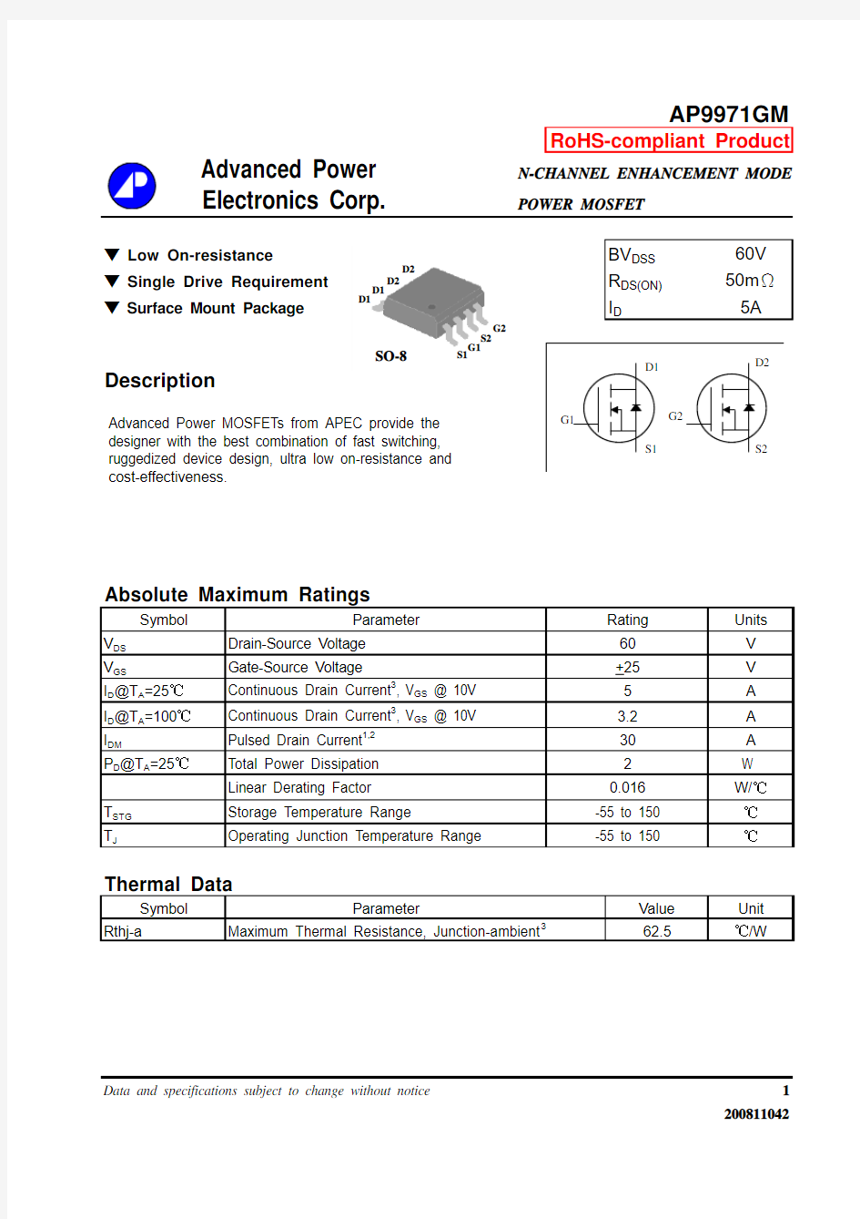
S1G1S2G2
D1
D1
D2D2
SO-8
Electrical Characteristics@T j =25o C(unless otherwise specified)
Symbol Parameter
Test Conditions
Min.Typ.
Max.Units BV DSS
Drain-Source Breakdown Voltage V GS =0V, I D =250uA 60--V ΔB V DSS /ΔT j
Breakdown Voltage Temperature Coefficient Reference to 25℃, I D =1mA
-0.06-V/℃R DS(ON)Static Drain-Source On-Resistance 2V GS =10V, I D =5A --50m ?V GS =4.5V, I D =2.5A --60m ?V GS(th)Gate Threshold Voltage V DS =V GS , I D =250uA 1-3V g fs Forward Transconductance
V DS =10V, I D =5A - 16 - S I DSS Drain-Source Leakage Current V DS =60V, V GS =0V --1uA Drain-Source Leakage Current (T j =70o C)V DS =48V ,V GS =0V
--25uA I GSS Gate-Source Leakage V GS = +25V --+100nA Q g Total Gate Charge 2I D =5A -32.5-nC Q gs Gate-Source Charge V DS =48V - 4.9-nC Q gd Gate-Drain ("Miller") Charge V GS =10V -8.8-nC t d(on)Turn-on Delay Time 2V DS =30V -9.6-ns t r Rise Time
I D =5A
-10-ns t d(off)Turn-off Delay Time R G =3.3Ω,V GS =10V -30-ns t f Fall Time R D =6Ω- 5.5-ns C iss Input Capacitance V GS =0V -1658-pF C oss Output Capacitance
V DS =25V -156-pF C rss
Reverse Transfer Capacitance
f=1.0MHz
-
109
-pF
Source-Drain Diode
Symbol Parameter
Test Conditions
Min.Typ.Max.Units V SD
Forward On Voltage 2I S =1.6A, V GS =0V -- 1.2V t rr
Reverse Recovery Time 2I S =5A, V GS =0V ,-29.2-ns Qrr
Reverse Recovery Charge
dI/dt=100A/μs
-48
-nC
Notes:
1.Pulse width limited by Max. junction temperature.
2.Pulse width <300us , duty cycle <2%.
3.Surface mounted on 1 in 2 copper pad of FR4 board ; 135℃/W when mounted on min. copper pad.
THIS PRODUCT IS SENSITIVE TO ELECTROSTATIC DISCHARGE, PLEASE HANDLE WITH CAUTION.
USE OF THIS PRODUCT AS A CRITICAL COMPONENT IN LIFE SUPPORT OR OTHER SIMILAR SYSTEMS IS NOT AUTHORIZED.APEC DOES NOT ASSUME ANY LIABILITY ARISING OUT OF THE APPLICATION OR USE OF ANY PRODUCT OR CIRCUIT DESCRIBED HEREIN; NEITHER DOES IT CONVEY ANY LICENSE UNDER ITS PATENT RIGHTS, NOR THE RIGHTS OF OTHERS.
APEC RESERVES THE RIGHT TO MAKE CHANGES WITHOUT FURTHER NOTICE TO ANY PRODUCTS HEREIN TO IMPROVE RELIABILITY, FUNCTION OR DESIGN.
2
AP9971GM
Fig 1. Typical Output Characteristics Fig 2. Typical Output Characteristics
Fig 3. On-Resistance v.s. Gate Voltage
Fig 4. Normalized On-Resistance v.s. Junction Temperature
Fig 6. Gate Threshold Voltage v.s.
Reverse Diode
Junction Temperature
3
Fig 7. Gate Charge Characteristics Fig 8. Typical Capacitance Characteristics
Fig 9. Maximum Safe Operating Area Fig 10. Effective Transient Thermal Impedance
Fig 11. Switching Time Waveform Fig 12. Gate Charge Waveform
AP9971GM
4
G