EE-SV3-B中文资料

Internal Circuit
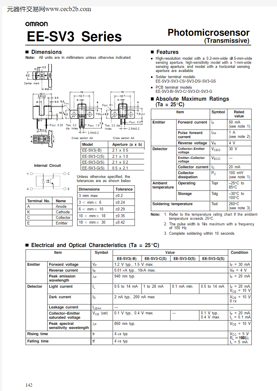
Model Aperture (a x b)EE-SV3(-B) 2.1 x 0.5EE-SV3-C(S)
2.1 x 1.0EE-SV3-D(S) 2.1 x 0.2EE-SV3-G(S)
0.5 x 2.1
Four, 1.5Four , 0.5
Four, R1
Four,R1
Two, 3.2dia. holes
Two, 3.2 dia.holes
Four , 0.25
Center mark
Cross section AA Cross section AA
2.54±0.2
2.54±0.2
142
Photomicrosensor
(Transmissive)
EE-SV3 Series
Note:
All units are in millimeters unless otherwise indicated.
?
High-resolution model with a 0.2-mm-wide or 0.5-mm-wide sensing aperture, high-sensitivity model with a 1-mm-wide sensing aperture, and model with a horizontal sensing aperture are available.
?
Solder terminal models:
EE-SV3/-SV3-CS/-SV3-DS/-SV3-GS ?
PCB terminal models
EE-SV3-B/-SV3-C/-SV3-D/-SV3-G
Absolute Maximum Ratings (Ta = 25°C)
Item
Symbol Rated value Emitter Forward current I F 50 mA
(see note 1)Pulse forward current
I FP 1 A
(see note 2)Reverse voltage
V R 4 V Detector
Collector–Emitter voltage
V CEO 30 V Emitter–Collector voltage
V ECO
---Collector current I C 20 mA Collector dissipation
P C 100 mW (see note 1)Ambient temperature
Operating Topr –25°C to 85°C Storage
Tstg –30°C to 100°C Soldering temperature Tsol
260°C
(see note 3)
Note:
1.Refer to the temperature rating chart if the ambient temperature exceeds 25°C.
2.The pulse width is 10 μs maximum with a frequency of 100 Hz.
https://www.360docs.net/doc/ce13393657.html,plete soldering within 10 seconds.
°C)
Item
Symbol
Value
Condition
EE-SV3(-B)
EE-SV3-C(S)
EE-SV3-D(S)
EE-SV3-G(S)
Emitter
Forward voltage V F 1.2 V typ., 1.5 V max.I F = 30 mA Reverse current I R 0.01 μA typ., 10 μA max.V R = 4 V Peak emission wavelength
λP 940 nm typ.I F = 20 mA Detector
Light current I L 0.5 to 14 mA
1 to 28 mA
0.1 mA min.
0.5 to 14 mA
I F = 20 mA,V CE = 10 V Dark current I D 2 nA typ., 200 nA max.V CE = 10 V ,0 ?x Leakage current I LEAK ------Collector–Emitter saturated voltage V CE (sat)0.1 V typ., 0.4 V max.---0.1 V typ., 0.4 V max.
I F = 20 mA,I L = 0.1 mA Peak spectral
sensitivity wavelength
λP 850 nm typ.V CE = 10 V Rising time tr 4 μs typ.V CC = 5 V ,=100Falling time
tf
4 μs typ.
R L = 100 ?,I L = 5 mA
143
Forward Current vs. Collector Dissipation Temperature Rating
Forward Current vs. Forward Voltage Characteristics (Typical)
Light Current vs. Forward Current
Characteristics (Typical)
Ambient temperature T a (°C)
C o l l e c t o r d i s s i p a t i o n P c (m W )
Forward voltage V F (V)
F F o r w a r d c u r r e n t I (m A )
F F o r w a r d c u r r e n t I (m A )
Forward current I F (mA)
L i g h t c u r r e n t I (m A )
L Light Current vs. Collector–Emitter Voltage Characteristics (EE-SV3(-B))
Relative Light Current vs. Ambi-ent Temperature Characteristics (Typical)
Dark Current vs. Ambient Temperature Characteristics (Typical)
Collector–Emitter voltage V CE (V)
L i g h t c u r r e n t I (m A )
L Ambient temperature T a (°C)
Ambient temperature T a (°C)
Response Time vs. Load Resis-tance Characteristics (Typical)
Sensing Position Characteristics (EE-SV3-D(S))
Load resistance R L (k ?)
Distance d (mm)Sensing Position Characteristics (EE-SV3(-B))
Distance d (mm)
Sensing Position Characteristics (EE-SV3-G(S))
Distance d (mm)Sensing Position Characteristics (EE-SV3-C(S))
Distance d (mm)
Ta = –30°C Ta = 25°C Ta = 70°C
I F = 20 mA
V CE = 5 V
V CE = 10 V
0 ?x
I F = 20 mA
V CE = 10 V Ta = 25°C
Vcc = 5 V
Ta = 25°C
Input Output
Input
Output
90 %10 %
Ta = 25°C V CE = 10 V
I F = 50 mA I F = 40 mA I F = 30 mA I F = 20 mA I F = 10 mA
Ta = 25°C
I F = 20 mA
V CE = 10 V Ta = 25°C
Center of optical axis
Center of optical axis
I F = 20 mA
V CE = 10 V Ta = 25°C
Center of optical axis
I F = 20 mA
V CE = 10 V Ta = 25°C
Center of optical axis
R e s p o n s e t i m e t r , t f ( s )R e l a t i v e l i g h t c u r r e n t I (%)L
D a r k c u r r e n t I (n A )D
μ
R e l a t i v e l i g h t c u r r e n t I (%)L
R e l a t i v e l i g h t c u r r e n t I (%)L
R e l a t i v e l i g h t c u r r e n t I (%)L
R e l a t i v e l i g h t c u r r e n t I (%)L
Response Time Measurement Circuit
I F Pc
d –
+