MIC94062YMT TR;MIC94060YC6 TR;MIC94061YC6 TR;MIC94063YMT TR;MIC94060YMT TR;中文规格书,Datasheet资料
MIC94060/61/62/63
High Side Power Switches
MLF and Micro LeadFrame are registered trademarks of Amkor Technologies, Inc.
General Description
The MIC94060-63 are high-side load switches designed for operation between 1.7V to 5.5V. The devices contain a low on-resistance P-channel MOSFET that supports over 2A of continuous current. The MIC94061and MIC94063 features an active load discharge circuit which insures capacitive loads retain no charge when the main switch is in an OFF state.
MIC94060-61 feature rapid turn on while MIC94062-63 provide a slew rate controlled Soft-Start turn-on of 800μs (typical) to prevent in-rush current from glitching supply rails.
An active pull-down on the enable input keeps MIC94060-63 in a default OFF state until the EN pin is pulled to a high level. Built-in level shift circuitry allows low voltage logic signals to switch higher supply voltages, or vice versa; high level logic signals can control low level voltages.
MIC94060-63’s operating voltage range makes them suitable for 1-cell Lithium ion and 2- to 3-cell NiMH/NiCad/Alkaline powered systems, as well as all 5V applications. Their low operating current of 2μA and low shutdown current of <1μA maximize battery life.
Data sheets and support documentation can be found on Micrel’s web site at: https://www.360docs.net/doc/d014792859.html,. Features
? 1.7V to 5.5V input voltage range ? 2A continuous operating current ? 77m ? (typ) R ON
? Built-in level shift for control logic; can be operated by 1.5V logic.
? Low 2μA quiescent current ? Soft-Start: MIC94062-63 ? Micro-power shutdown <1μA
? Load discharge circuit: MIC94061, MIC94063 ? Space saving 1.2x1.6 mm Thin MLF ? package
Applications
? Load switch in portable applications: - Cellular phones - PDAs - MP3 players - Digital Cameras - Portable instrumentation ? Battery switch-over circuits ? Level translator
________________________________________________________________________________________________________
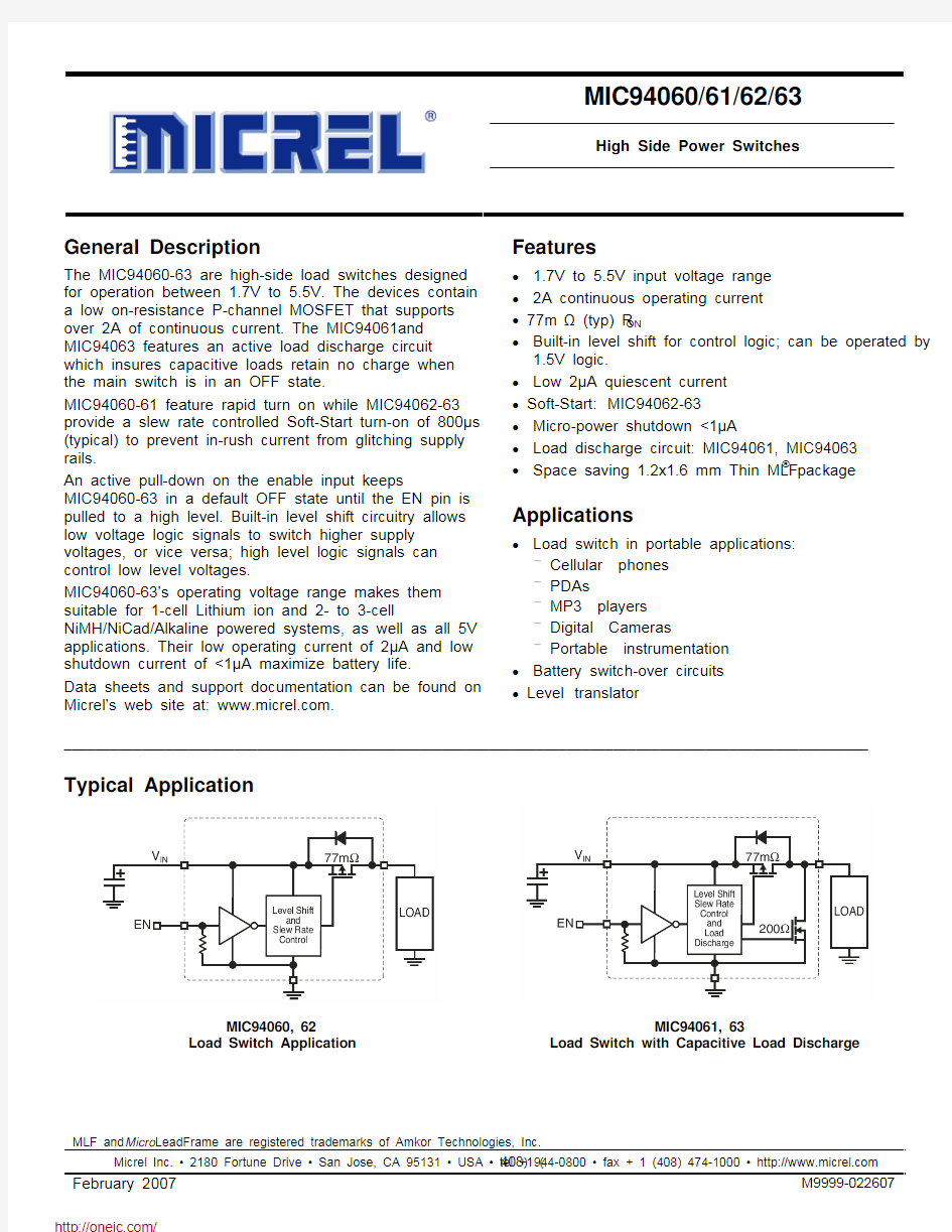
Typical Application
MIC94060, 62
Load Switch Application
MIC94061, 63
Load Switch with Capacitive Load Discharge
Ordering Information
Part Number
Part Marking (1)
Standard Pb-Free Standard Pb-Free Soft-Start Load Discharge Package
MIC94060BC6 MIC94060YC6 P54 P54 MIC94061BC6 MIC94061YC6 P55 P55 ● MIC94062BC6 MIC94062YC6 P56 P56 ● MIC94063BC6 MIC94063YC6
P57 P57 ● ● SC-70-6
— MIC94060YMT — P54 — MIC94061YMT — P55 ● — MIC94062YMT — P56 ● —
MIC94063YMT
—
P57
●
●
1.2mm x 1.6mm
Thin MLF ?
Notes
1. Underbar symbol on SC-70 Pb-free packages may not be to scale.
Pin Configuration
SC-70-6 (C6)
1.2x1.6 mm Thin MLF ? (MT)
Pin Description
Pin Number SC-70 MLF Pin Name Pin Function
1 1 V OUT Drain of P-channel MOSFET.
2,5
2
GND Ground and the backside pad (MLF only) should both be connected to electrical ground. 4 3 V IN Source of P-channel MOSFET.
3 4 EN Enable (Input): Active-high CMOS compatible control input for switch A. Do not leave floating.
6 --
NIC
No Internal Connection. A signal or voltage applied to this pin will have no effect on device operation.
Absolute Maximum Ratings (1)
Input Voltage (V IN )................................................+6V Enable Voltage (V EN ) ...........................................+6V Continuous Drain Current (I D ) (3) T A = 25°C.......................................................±2A T A = 85°C....................................................±1.4A Pulsed Drain Current (I DP ) (4)................................±6A Continuous Diode Current (I S ) (4).....................–50mA Storage Temperature (T s )...............–55°C to +150°C EDS Rating – HBM (6)..........................................4KV
Operating Ratings (2)
Input Voltage (V IN ).................................+1.7 to +5.5V Junction Temperature (T A )..............–40°C to +125°C Package Thermal Resistance SC-70-6 (θJA ).........................................240°C/W 1.2x1.6 MLF (θJA )..................................172°C/W 1.2x1.6 MLF (θJC ) (3)..............................134°C/W
Electrical Characteristics
V IN = 5V; T A = 25°C, bold values indicate –40°C< T A < +85°C, unless noted. Symbol Parameter Condition
Min Typ Max Units V IN = 1.8V to 4.5V, I D = –250μA 0.5 1.2 V V EN_TH Enable Threshold Voltage V IN = 1.7V to 4.5V, I D = –250μA 0.4 1.2 V I EN Enable Input Current V IN = V EN = 5.5V
2 4 μA I VIN OFF State Leakage Current V IN = +5.5V, V EN = 0V
1 μA V IN = +4.5V, ID = –100mA, V EN = 1.5V 77 110 m ? V IN = +3.6V, ID = –100mA, V EN = 1.5V 85 115 m ? V IN = +2.5V, ID = –100mA, V EN = 1.5V 100 140 m ? V IN = +1.8V, ID = –100mA, V EN = 1.5V 145 200 m ? R DS(ON)
P-Channel Drain to Source ON Resistance
SC-70 Package
V IN = +1.7V, ID = –100mA, V EN = 1.5V
155 215 m ? V IN = +4.5V, ID = –100mA, V EN = 1.5V 85 115 m ? V IN = +3.6V, ID = –100mA, V EN = 1.5V 100 140 m ? V IN = +2.5V, ID = –100mA, V EN = 1.5V 145 200 m ? V IN = +1.8V, ID = –100mA, V EN = 1.5V 155 215 m ? R DS(ON)
P-Channel Drain to Source ON Resistance
MLF Package
V IN = +1.7V, ID = –100mA, V EN = 1.5V
165
225
m ?
R SHUTDOWN Turn-Off Resistance
V IN = +3.6V, I TEST = 1mA, V EN = 0V MIC94061, 63
200 300 ?
Dynamic
Symbol Parameter Condition
Min Typ Max Units V IN = +3.6V, ID = –100mA, V EN = 1.5V MIC94060, 61
0.85 1.5 μs
t ON_DLY
Turn-On Delay Time
V IN = +3.6V, ID = –100mA, V EN = 1.5V MIC94062, 63
700 1200 μs V IN = +3.6V, ID = –100mA, V EN = 1.5V MIC94060, 61
0.5 1 5 μs t ON_RISE
Turn-On Rise Time
V IN = +3.6V, ID = –100mA, V EN = 1.5V MIC94062, 63
500 800 1500 μs
Dynamic (cont.)
V IN = +3.6V, ID = –100mA, V EN = 1.5V MIC94060, 61 100 200 ns
t OFF_DLY Turn-Off Delay Time
V IN = +3.6V, ID = –100mA, V EN = 1.5V
MIC94062, 63
60 200 ns
V IN = +3.6V, ID = –100mA, V EN = 1.5V MIC94060, 61 60 100 ns
t OFF_FALL Turn-Off Fall Time
V IN = +3.6V, ID = –100mA, V EN = 1.5V
MIC94062, 63
60 100 ns
Notes:
1. Exceeding the absolute maximum rating may damage the device.
2. The device is not guaranteed to function outside its operating rating.
3. With backside thermal contact to PCB.
4. Pulse width <300μs with < 2% duty cycle.
5. Continuous body diode current conduction (reverse conduction, i.e. V OUT to V IN) is not recommended.
6. Devices are ESD sensitive. Handling precautions recommended. HBM (Human body model), 1.5k in series with 100pF.
Typical Characteristics
Functional Characteristics MIC94060
Package Information
6-Pin SC-70 (C6)
4-Pin Thin MLF? (MT)
分销商库存信息:
MICREL
MIC94062YMT TR MIC94060YC6 TR MIC94061YC6 TR MIC94063YMT TR MIC94060YMT TR MIC94061YMT TR MIC94060BC6 TR MIC94061BC6 TR MIC94062BC6TX