W3DG72128V-D1中文资料

1GB - 128Mx72 SDRAM, UNBUFFERED w/PLL
FEATURES
PC100 and PC133 compatible Burst Mode Operation
Auto and Self Refresh capability LVTTL compatible inputs and outputs Serial Presence Detect with EEPROM
Fully synchronous: All signals are registered on the positive
edge of the system clock
Programmable Burst Lengths: 1, 2, 4, 8 or Full Page 3.3V ± 0.3V Power Supply 144 Pin SO-DIMM JEDEC
DESCRIPTION
The W3DG72128V is a 128Mx72 synchronous DRAM module which consists of nine 128Mx8 stacks of SDRAM components in TSOP II package, and one 2Kb EEPROM in an 8 pin TSSOP package for Serial Presence Detect which are mounted on a 144 pin SO -DIMM multilayer FR4 Substrate. This module is structured as 2 Ranks of 64Mx72 SDRAM.
* T his product is under development, is not quali? ed or characterized and is subject to change without notice..
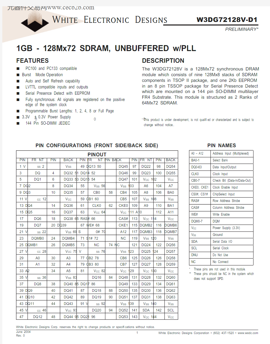
PIN CONFIGURATIONS (FRONT SIDE/BACK SIDE)PIN NAMES
* These pins are not used in this module.
** These pins should be NC in the system which does not support SPD.
A0 – A12Address Input (Multiplexed)BA0-1Select Bank DQ0-63Data Input/Output CLK0Clock Input
CB0-7Check Bit (Data-In/Data-Out)CKE0, CKE1Clock Enable Input CS0#, CS1#ChipSelect Input RAS#Row Address Strobe CAS#Column Address Strobe WE#Write Enable DQM0-7DQM
V CC Power Supply (3.3V)V SS Ground SDA Serial Data I/O SCL Serial Clock DNU Do Not Use NC
No Connect
PINOUT
PIN FR O NT PIN BACK PIN FR O NT PIN BACK PIN FR O NT PIN BACK 1 V SS 2 V SS 49 DQ13 50 DQ45 97 DQ22 98 DQ543 DQ
4 DQ32 51 DQ14 52 DQ46 99 DQ23 100 DQ55
5
DQ1 6 DQ33 53 DQ15 54 DQ47 101 V CC 102 V CC
7 DQ2 8 DQ34 55 V SS 56 V SS 103 A6 104 A79 DQ3 10 DQ35 57 CB0 58 CB4 105 A8 106 BA011 V CC 12 V CC 59 CB1 60 CB5 107 V SS 108 V SS 13 DQ4 14 DQ36 61 CLK0 62 CKE0 109 A9 110 BA115 DQ5 16 DQ37 63 V CC 64 V CC 111 A10 112 A1117 DQ6 18 DQ38 65 RAS# 66 CAS# 113 V CC 114 V CC 19 DQ7 20 DQ39 67 WE# 68 CKE1 115 DQMB2 116 DQMB621 V SS 22 V SS 69 S 0# 70 A12 117 DQMB3 118 DQMB723 DQMB0 24 DQMB4 71 S1# 72 NC 119 V SS 120 V SS 25 DQMB1 26 DQMB5 73 NC 74 NC 121 DQ24 122 DQ5627 V CC 28 V CC 75 V SS 76 V SS 123 DQ25 124 DQ5729 A0 30 A3 77 CB2 78 CB6 125 DQ26 126 DQ5831 A1 32 A4 79 CB3 80 CB7 127 DQ27 128 DQ5933 A2 34 A5 81 V CC 82 V CC 129 V CC 130 V CC 35 V SS 36 V SS 83 DQ16 84 DQ48 131 DQ28 132 DQ6037 DQ8 38 DQ40 85 DQ17 86 DQ49 133 DQ29 134 DQ6139 DQ9 40 DQ41 87 DQ18 88 DQ50 135 DQ30 136 DQ6241 DQ10 42 DQ42 89 DQ19 90 DQ51 137 DQ31 138 DQ6343 DQ11 44 DQ43 91 V SS 92 V SS 139 V SS 140 V SS 45 V CC 46 V CC 93 DQ20 94 DQ52 141 SDA 142 SCL 47 DQ12 48 DQ44 95 DQ21 96 DQ53 143 V CC 144 V CC
ABSOLUTE MAXIMUM RATINGS
Note: Permanent device damage may occur if “ABSOLUTE MAXIMUM RATINGS”V are exceeded. Functional operation should be restricted to recommended operating condition. Exposure to higher than recommended voltage for extended periods of time could affect device reliability.
RECOMMENDED DC OPERATING CONDITIONS
(Voltage Referenced to: V SS = 0V, T A = 0°C ≤ +70°C)
Note: 1. V IH (max)= 5.6V AC. The overshoot voltage duration is ≤ 3ns. 2. V IL (min)= -2.0V AC. The undershoot voltage duration is ≤ 3ns. 3. Any input 0V ≤ V IN ≤ V CCQ Input leakage currents include Hi-Z output leakage for all bi-directional buffers with Tri-State outputs.
CAPACITANCE
(T A = 25°C, f = 1MHz, V CC = 3.3V, V REF =1.4V ± 200mV)
Parameter
Symbol Value Units Voltage on any pin relative to V SS V IN , V OUT -1.0 ~ 4.6V Voltage on V CC supply relative to V SS V CC , V CCQ -1.0 ~ 4.6V Storage Temperature T STG -55 ~ +150
°C Power Dissipation P D 18 W
Short Circuit Current
I OS
50
mA
Parameter Symbol Min Typ Max Unit Note
Supply Voltage V CC 3.0 3.3 3.6
V Input High Voltage V IH 2.0 3.0V CCQ+0.3V 1Input Low Voltage V IL -0.3—0.8V 2Output High Voltage V OH 2.4——V I OH = -2mA Output Low Voltage V OL ——0.4V I OL = -2mA
Input Leakage Current
I LI
-10
—
10
μA
3Parameter
Symbol Max Unit Input Capacitance (A0-A12)C IN115pF Input Capacitance (RAS#,CAS#,WE#)C IN215pF Input Capacitance (CKE0)C IN315pF Input Capacitance (CLK0)C IN420pF Input Capacitance (CS0#)C IN515pF Input Capacitance (DQM0-DQM7)C IN615pF Input Capacitance (BA0-BA1)
C IN715pF Data Input/Output Capacitance (DQ0-DQ63)Cou T 22pF Data Input/Output Capacitance (CB0-7)
Cou T1
22
pF
OPERATING CURRENT CHARACTERISTICS (V CC = 3.3V, T A = 0°C to +70°C)
Notes: 1. Measured with outputs open.
2. Refresh period is 64ms.Version
Parameter Symbol Conditions133100Units Note
Operating Current (One bank active)I CC1Burst Length = 1
t RC ≥ t RC(min)
I OL = 0mA
1,8901,710mA1
Precharge Standby Current in Power Down Mode I CC2P CKE ≤ V IL(max), t CC = 10ns145mA I CC2PS CKE & CLK ≤V IL(max), t CC = ∞135
Precharge Standby Current in Non-Power Down Mode I CC2N CKE ≥V IH(min), CS ≥ V IH(min), tcc =10ns
Input signals are charged one time during 20360
mA I CC2NS CKE ≥ V IH(min), CLK ≤ V IL(max), t CC = ∞
Input signals are stable180
Active Standby Current in Power-Down Mode I CC3P CKE ≥ V IL(max), t CC = 10ns180mA I CC3PS CKE & CLK ≤V IL(max), t CC = ∞130
Active Standby Current in Non-Power Down Mode I CC3N CKE ≥ V IH(min), CS ≥ V IH(min), tcc = 10ns Input
signals are changed one time during 20ns
540mA
I CC3NS CKE ≥ V IH(min), CLK ≤ V IL(max), tcc = ∞
Input signals are stable
405mA
Operating Current (Burst mode)I CC4Io = mA
Page burst
4 Banks activated
t CCD = 2CLK
1,8901,620mA1
Refresh Current I CC5t RC ≥ t RC(min)3,0602,880mA2 Self Refresh Current I CC6CKE ≤ 0.2V130mA
PACKAGE DIMENSIONS FOR D1
Ordering Information Speed CAS Latency Height* W3DG72128V10D1100MHz CL=231.75 (1.250”) W3DG72128V7D1133MHz CL=231.75 (1.250”) W3DG72128V75D1133MHz CL=331.75 (1.250”) Note: For industrial temperature range product, add an "I" to the end of the part number.
PACKAGE DIMENSIONS FOR D1
* ALL DIMENSIONS ARE IN MILLIMETERS AND (INCHES).
Document Title
1GB - 128Mx72 SDRAM, UNBUFFERED w/PLL
Revision History
Rev #History Release Date Status Rev 0Created Datasheet6-03Advanced
6-04Preliminary Rev 1 1.1 Updated Datasheet (CAP and I DD specs)
1.2 Removed “ED” from part number