铁酸铋的漏电流机制

Leakage mechanisms in BiFeO3 thin films
Gary W. Pabst, Lane W. Martin, Ying-Hao Chu, and R. Ramesh
Citation: Appl. Phys. Lett. 90, 072902 (2007); doi: 10.1063/1.2535663
View online: https://www.360docs.net/doc/567764445.html,/10.1063/1.2535663
View Table of Contents: https://www.360docs.net/doc/567764445.html,/resource/1/APPLAB/v90/i7
Published by the American Institute of Physics.
Related Articles
Large photoinduced conductivity reduction in thin films of metallic ferromagnetic manganites
Appl. Phys. Lett. 99, 222507 (2011)
Temperature-dependent leakage current behavior of epitaxial Bi0.5Na0.5TiO3-based thin films made by pulsed laser deposition
J. Appl. Phys. 110, 103710 (2011)
Probing the metal-insulator transition of NdNiO3 by electrostatic doping
Appl. Phys. Lett. 99, 192107 (2011)
Evidence of interface conversion and electrical characteristics improvement of ultra-thin HfTiO films upon rapid thermal annealing
Appl. Phys. Lett. 99, 182904 (2011)
Examination of insulator regime conduction mechanisms in epitaxial and polycrystalline SmNiO3 thin films
J. Appl. Phys. 110, 094102 (2011)
Additional information on Appl. Phys. Lett.
Journal Homepage: https://www.360docs.net/doc/567764445.html,/
Journal Information: https://www.360docs.net/doc/567764445.html,/about/about_the_journal
Top downloads: https://www.360docs.net/doc/567764445.html,/features/most_downloaded
Information for Authors: https://www.360docs.net/doc/567764445.html,/authors
Leakage mechanisms in BiFeO 3thin ?lms
Gary W.Pabst,Lane W.Martin,a ?Ying-Hao Chu,and R.Ramesh
Department of Materials Science and Engineering,University of California,Berkeley,Berkeley,California 94720and Lawrence Berkeley National Laboratory,Berkeley,California 94720
?Received 18December 2006;accepted 13January 2007;published online 13February 2007?The authors report results of transport studies on high quality,fully epitaxial BiFeO 3thin ?lms grown via pulsed laser deposition on SrRuO 3/DyScO 3?110?substrates.Ferroelectric tests were conducted using symmetric and asymmetric device structures with either SrRuO 3or Pt top electrodes and SrRuO 3bottom https://www.360docs.net/doc/567764445.html,parison between these structures demonstrates the in?uence of electrode selection on the dominant transport mechanism.Analysis of ?lm electrical response suggests Poole-Frenkel emission as the limiting leakage current mechanism in the symmetric structure.Temperature dependent measurements yield trap ionization energies of ?0.65–0.8eV.No clear dominant leakage mechanism was observed for the asymmetric structure.?2007American Institute of Physics .?DOI:10.1063/1.2535663?
With an ever-expanding demand for data storage,trans-ducers,and microelectromechanical systems applications,materials with superior ferroelectric and piezoelectric re-sponses are of great interest.The Pb ?Zr,Tr ?O 3?PZT ?family of materials has served as the cornerstone of these devices to date.A critical drawback of this material,however,is its toxicity due to the lead content.Recently,lead-free ferroelec-tric BiFeO 3?BFO ?has attracted a great deal of attention because of its superior properties in both epitaxial and polycrystalline thin ?lms.1–4Its remnant polarization P r and out-of-plane converse piezoelectric coef?cient d 33are com-parable to those of the tetragonal,Ti-rich PZT system.More-over,due to a high Curie temperature ?T C =820–850°C ?,5,6it also shows great promise for use in high temperature ap-plications.Additionally,previous studies have successfully integrated BFO ?lms on Si substrates by using a SrTiO 3?STO ?template layer and SrRuO 3?SRO ?bottom electrode.7,8These ?lms exhibited large coercive ?elds and a large leak-age current,which might limit the applicability of BFO in devices.Such drawbacks have prompted a number of studies attempting to reduce the leakage in BFO through the use of chemical dopants.9–12In fact,Fujitsu Microelectronics America,Inc.recently announced the production of 65nm ferroelectric random access memory devices using Mn-doped BFO to reduce the leakage current.13In this letter we focus our attention on the mechanisms that lead to the large leakage current in high quality BFO thin ?lms.This will,in turn,help guide future work to integrate BFO into functional microelectronic devices.
Thin ?lm heterostructures of BFO ??175nm ?and SRO ??50nm ?were grown on DyScO 3?DSO ??110?single crys-tal substrates via pulsed laser deposition at 700°C and 100mTorr partial pressure of oxygen.X-ray diffraction ?Panalytical X’Pert MRD Pro ?shows that BFO ?lms grown on DSO substrates are single phase and exhibit very narrow rocking curves for the 002-pseudocubic diffraction peak of BFO ?full width at half maximum ?of 0.055°pointing to the extremely high quality and epitaxial nature of these ?lms.Additionally,at these thicknesses,the BFO ?lms appear to
relax to a derivative of the bulk rhombohedral structure 14as con?rmed by a ?scan of the rhombohedrally nondegenerate 210R re?ection in BFO.15,16Note that we do not rule out an additional slight monoclinic distortion to the lattice.Through careful control of the growth of the underlying SRO bottom electrode layer,we can engineer the structural domain con-?guration of the SRO and thereby affect control over the BFO domain structure.17The samples measured here exhibit multivariant domain structures in the BFO ?lms as imaged via piezoforce microscopy ?not shown here ?.Top SRO elec-trodes ?32?m diameter ?were deposited ex situ at room tem-perature and then annealed in oxygen at 600°C for 30min to facilitate crystallization.Finally,approximately 150nm of platinum was sputtered onto the SRO top electrodes to facili-tate a low resistance contact.Ferroelectric and leakage mea-surements were carried out using a Radiant Technologies Inc.RT6000S ferroelectric test system.
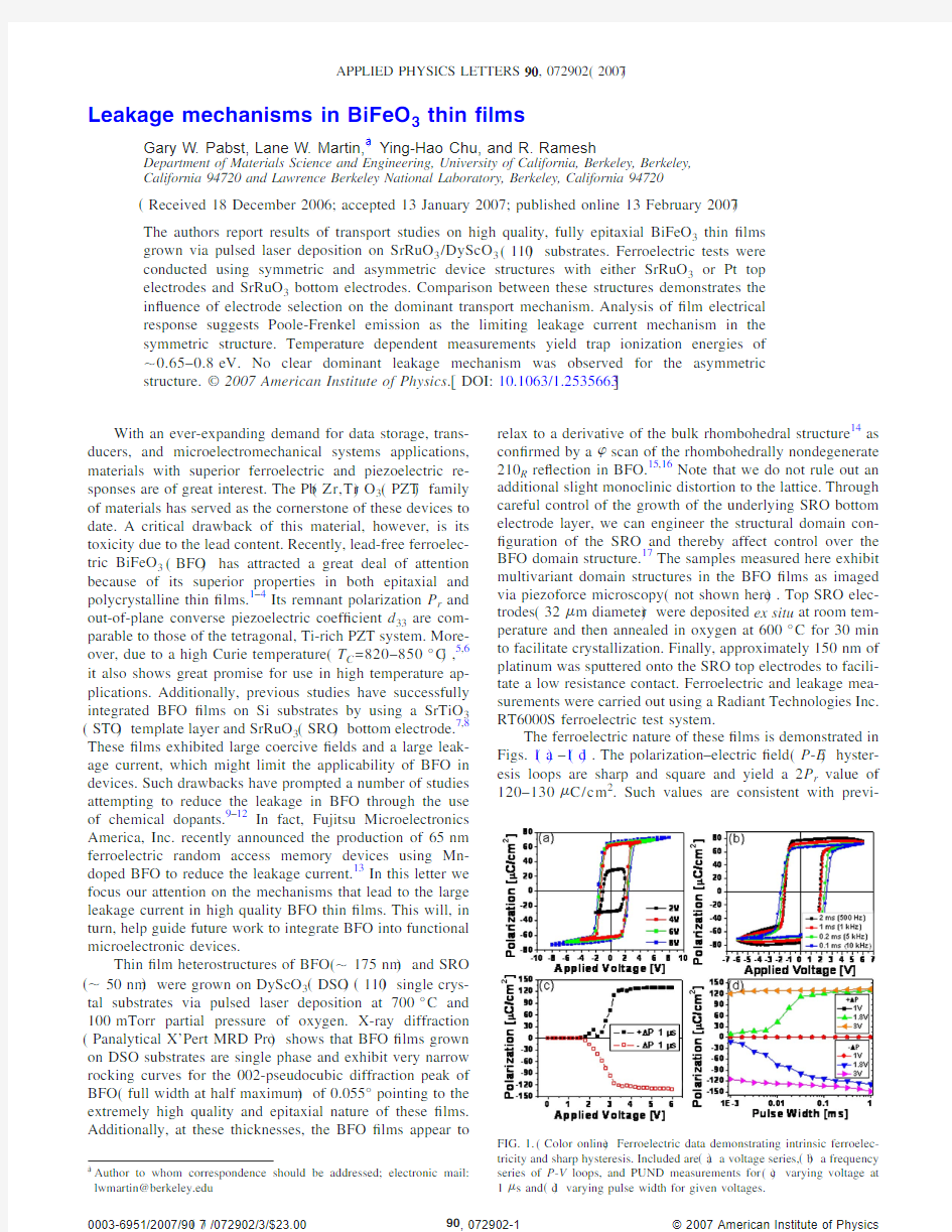
The ferroelectric nature of these ?lms is demonstrated in Figs.1?a ?–1?d ?.The polarization–electric ?eld ?P -E ?hyster-esis loops are sharp and square and yield a 2P r value of 120–130?C/cm 2.Such values are consistent with previ-
a ?
Author to whom correspondence should be addressed;electronic mail:
lwmartin@https://www.360docs.net/doc/567764445.html,
FIG.1.?Color online ?Ferroelectric data demonstrating intrinsic ferroelec-tricity and sharp hysteresis.Included are ?a ?a voltage series,?b ?a frequency series of P -V loops,and PUND measurements for ?c ?varying voltage at 1?s and ?d ?varying pulse width for given voltages.
APPLIED PHYSICS LETTERS 90,072902?2007?
0003-6951/2007/90?7?/072902/3/$23.00?2007American Institute of Physics
90,072902-1
ously measured values for BFO grown on STO and STO/Si substrates.1,7,8,15The saturation of the hysteresis loops as a function of voltage?Fig.1?a??is key evidence of intrinsic ferroelectricity in the?lms.The weak frequency dependence of the loops?Fig.1?b??also supports this claim.To more closely investigate the ferroelectric properties,pulsed polar-ization positive up negative down?PUND?measurements were made with a varying?eld at a pulse width of1?s?Fig. 1?c??and with a varying pulse width at?xed voltages?Fig. 1?d??.The switched polarization values??P?of these mea-surements match well with the2P r values obtained from the P-E loops.Note also the weak pulse width dependence of Fig.1?d?once saturation is reached,yet another indication of robust intrinsic ferroelectricity.
The literature on possible leakage current limiting mechanisms for BFO and other similar ferroelectric perov-skite oxides discusses a large number of possible mecha-nisms.These mechanisms fall into two categories,bulk-limited and interface-limited conduction.Of all the possible mechanisms,we consider three in this letter that are com-monly observed in other perovskite oxides.The?rst mecha-nism is interface-limited Schottky emission,which arises from a difference in Fermi levels between a metal?electrode?and an insulator or semiconductor??lm?.The energy differ-ence creates a potential barrier between the metal and insu-lator that charges must overcome.The current density across a Schottky barrier is18
J S=AT2exp???k B T?1k B T ?q3V4??o Kd?1/2?,?1?
where A is the Richardson constant,?is the height of the Schottky barrier,K is the dielectric constant of the?lm,and d is the sample thickness.The second mechanism considered is bulk-limited space-charge-limited conduction?SCLC?. The limitation arises from a current impeding space charge forming as charges are injected into the?lm from the elec-trode at a rate faster than they can travel through the?lm. The current density for SCLC is19,20
J SCLC=9??o K
8
V2
d3
,?2?
where?is carrier mobility.The third mechanism is bulk-limited Poole-Frenkel emission.This conduction mechanism involves the consecutive hopping of charges between defect trap centers.The ionization of the trap charges can be both thermally and?eld activated.The conductivity for Poole-Frenkel emission is21
?PF=c exp??E I k B T?1k B T ?q3V??o Kd?1/2?,?3?
where c is a constant and E I is the trap ionization energy.
Typical leakage data?I-V?as a function of applied volt-age for a175nm thick?lm are shown in Fig.2?a?.Data for both positive and negative biases have been graphed on the same axis.By plotting our data in various manners as a func-tion of voltage,we can quickly gain insight into the nature of the leakage mechanism.According to Eq.?2?above,SCLC can be investigated by plotting the leakage data as J vs V2,as shown in Fig.2?b?.If SCLC were the dominant leakage mechanism,a straight?t to the data in Fig.2?b?would be possible.Since it shows an exponential trend,SCLC can be ruled out as the leakage current limiting mechanism for these BFO thin?lms for the voltage range measured.
Similar analysis of Eqs.?1?and?3?tells us that if a Schottky barrier controls the leakage current or if Poole-Frenkel emissions are dominant,semilog plots of J/T2vs V1/2and?vs V1/2,respectively,will show straight line?ts to the data.Both these plots,however,will often show regions with straight?ts to the data,as shown in Figs.2?c?and2?d?. To identify which mechanism might be dominating the leak-age current,it is necessary to extract the dielectric constant from the slopes of these plots.Iakovlev et al.report the index of refraction for BFO to be n=2.5;22thus we should expect a dielectric constant of K=n2=6.25.
From the Schottky plot?Fig.2?c??,a dielectric constant of?0.77is obtained for a negative bias as well as for?elds above?2V for a positive bias.The Poole-Frenkel plot ?Fig.2?d??on the other hand yields a dielectric constant of ?6.25for a negative bias and a positive bias above?2V.
Since this is the expected value of the dielectric constant and the value obtained from the Schottky plot is off by an order of magnitude,it is indicative of the leakage mechanism in these BFO?lms being dominated by Poole-Frenkel emis-sions.This is not unexpected as Poole-Frenkel emission has been identi?ed as the dominant leakage mechanism in other ferroelectric perovskites such as PZT.23,24In the case of BFO,the likely trap center is the Fe ions.It is widely ac-cepted that oxygen vacancies formed during growth cause a portion of the Fe3+ions to become Fe2+.These Fe ions are often considered to be responsible for the high leakage of BFO.
To determine the value of the Poole-Frenkel trap ioniza-tion energy we measured leakage as a function of tempera-ture.Plots of?vs1000/T for?xed voltages are shown in Fig.3?a?.From these slopes,ionization energies are ex-tracted and used to extrapolate the zero-?eld ionization en-ergy?Fig.3?b??.The low voltages not conforming to the trend are not unexpected as we do not observe Poole-Frenkel dominating in positive bias at low?elds.Fitting with the higher?eld data points yields a trap ionization energy of ?0.8eV.It should be noted,however,that multiple
mea-FIG.2.?Color online?Typical I-V characteristics of the Pt/SRO/BFO/SRO/ DSO thin?lm structures.?a?Typical leakage data.Various?ts of these data are shown to help determine the leakage mechanism:?b?SCLC,?c?Schottky barrier,or?d?Poole-Frenkel emission.
surements yielded a range of about 0.65–0.8eV for the trap ionization energy.
In contrast,analysis of data taken with Pt top electrodes ?Pt/BFO/SRO//DSO ?yielded inclusive results.Figure 4shows data for Pt analogous to that of Fig.2for the Pt/SRO top electrodes.First,notice that there is a considerable asym-metry between I -V behavior for positive and negative biases ?Fig.4?a ??,consistent with the fact that the top ?Pt ?and bot-tom ?SRO ?electrodes have different work functions and electron af?nities.Both polarities were prepoled and the re-sponse was repeatable.At this time the origin of this behav-ior is unknown.The SCLC,Schottky,and Poole-Frenkel plots all show regions with reasonable ?ts ?Figs.4?b ?and 4?c ??.The SCLC plot shows a linear ?t above ?2.5V for increasing negative bias ?Fig.4?b ??.This same region,how-ever,also shows a near perfect match for Schottky emission ?Fig.4?c ??.The higher voltage regions of both positive and the decreasing negative biases show linear ?ts for the Poole-Frenkel mechanism as well ?Fig.4?c ??.The best Poole-Frenkel ?t yields a dielectric constant of 5.5,which is slightly lower than the expected 6.25but not unreasonable.
These data indicate that using Pt alone as a top electrode to contact BFO ?lms creates a capacitor with competing leak-age mechanisms.
In summary,we have shown the leakage mechanism of BFO with symmetric SRO electrodes on DSO substrates to be dominated by Poole-Frenkel emission.A measured trap ionization energy of 0.65–0.8eV may correspond to the ion-ization of Fe 2+ions.We have also shown that there is no clear dominant mechanism when Pt is used as the top elec-trode.Careful studies and attention must be given to choose a contact with the appropriate material properties to alleviate this effect.
This work is supported by the Director,Of?ce of Basic Energy Sciences,Materials Sciences Division of the U.S.Department of Energy under Contract No.DE-AC02-05CH11231and ONR-MURI Grant No.E21-6RU-G4.
1
J.Wang,J.B.Neaton,H.Zheng,V .Nagarajan,S.B.Ogale,B.Liu,D.Viehland,V .Vaithyanathan, D.G.Schlom,U.V .Waghmare,N. A.Spaldin,K.M.Rabe,M.Wuttig,and R.Ramesh,Science 299,1719?2003?.2
W.Eerenstein,F.D.Morrison,J.Dho,M.G.Blamire,J.F.Scott,and N.D.Mathur,Science 307,1203?2005?.3
J.Wang,A.Scholl,H.Zheng,S.B.Ogale,D.Viehland,D.G.Schlom,N.A.Spaldin,K.M.Rabe,M.Wuttig,L.Mohaddes,J.Neaton,U.Waghmare,T.Zhao,and R.Ramesh,Science 307,5713?2005?.4
K.Y .Yun,M.Noda,and M.Okuyama,Appl.Phys.Lett.83,3981?2003?.5
Y .N.Venevtsev,G.Zhadanov,and S.Solov’ev,Sov.Phys.Crystallogr.4,538?1960?.6
G.Smolenskii,V .Isupov,A.Agranovskaya,and N.Kranik,Sov.Phys.Solid State 2,2651?1961?.7
J.Wang,H.Zheng,Z.Ma,S.Prasertchoung,M.Wuttig,R.Droopad,J.Yu,K.Eisenbeiser,and R.Ramesh,Appl.Phys.Lett.85,2574?2004?.8
S.Y .Yang,F.Zavaliche,L.Mohaddes-Ardabili,V .Vaithyanathan,D.G.Schlom,Y .J.Lee,Y .H.Chu,M.P.Cruz,Q.Zhan,T.Zhao,and R.Ramesh,Appl.Phys.Lett.87,102903?2005?.9
C.Wang,M.Takahashi,H.Fujino,X.Zhao,E.Kume,T.Horiuchi,and S.Sakai,J.Appl.Phys.99,054104?2006?.10
C.-F.Chung,J.-P.Lin,and J.-M.Wu,Appl.Phys.Lett.88,242909?2006?.11
G.L.Yuan and S.W.Or,Appl.Phys.Lett.88,062905?2006?.12
X.Qi,J.Dho,R.Tomov,M.G.Blamire,and J.L.MacManus-Driscoll,Appl.Phys.Lett.86,062903?2005?.13
Fujitsu Microelectronics America,Inc.,Sunnyvale,CA,Press Release,2August 2006?https://www.360docs.net/doc/567764445.html,/ca/en/news/pr/fma_20060802.html ?.14
F.Kubel and H.Schmid,Acta Crystallogr.,Sect.B:Struct.Sci.46,698?1990?.15
R.R.Das,D.H.Kim,S.H.Baek,C.B.Eom,F.Zavaliche,S.Y .Yang,R.Ramesh,Y .B.Chen,X.Q.Pan,X.Ke,M.S.Rzchowski,and S.K.Streiffer,Appl.Phys.Lett.88,242904?2006?.16
G.Xu,H.Hiraka,G.Shirane,J.Li,J.Wang,and D.Viehland,Appl.Phys.Lett.86,182905?2005?.17
Y .-H.Chu,Q.Zhan,L.W.Martin,M.P.Cruz,P.-L.Yang,G.W.Pabst,F.Zavaliche,S.-Y .Yang,J.-X.Zhang,L.-Q.Chen,D.G.Schlom,I.-N.Lin,T.-B.Wu,and R.Ramesh,Adv.Mater.?Weinheim,Ger.?18,2307?2006?.18
W.Schottky,Naturwiss.26,843?1938?.19
N.F.Mott and R.W.Gurney,Electronic Processes in Ionic Crystals ?Clarendon,Oxford,1940?.20
https://www.360docs.net/doc/567764445.html,mpert and P.Mark,Current Injection in Solids ?Academic,New York,1970?.21
J.Frenkel,https://www.360docs.net/doc/567764445.html,SR 5,685?1938?.22
S.Iakovlev,C.-H.Solterbeck,M.Kuhnke,and M.Es-Souni,J.Appl.Phys.97,094901?2005?.23
B.Nagaraj,S.Aggarwal,T.K.Song,T.Sawhney,and R.Ramesh,Phys.Rev.B 59,16022?1999?.24
P.Zubko,D.J.Jung,and J.F.Scott,J.Appl.Phys.100,114113?2006?
.
FIG.3.?Color online ??a ?Temperature dependence of conductivity with linear ?ts ?red lines ?used to extract trap ionization energies.?b ?Plot of trap ionization energies from ?a ?in order to extrapolate the zero-?eld trap ion-ization
energy.
FIG.4.?Color online ?Typical I -V characteristics of the Pt/BFO/SRO/DSO thin ?lm structures.?a ?Typical leakage data.Various manipulations of these data are shown to help determine the leakage mechanism:?b ?SCLC,?c ?Schottky barrier,or ?d ?Poole-Frenkel emission.
磁控溅射法制备薄膜材料综述
磁控溅射法制备薄膜材料综述 摘要薄膜材料的厚度是从纳米级到微米级,具有尺寸效应,在国防、通讯、航空、航天、电子工业等领域有着广泛应用,其有多种制造方法,目前使用较多的是溅射法,其中磁控溅射的应用较为广泛。本文主要介绍了磁控溅射法的原理、特点,以及制备过程中基片温度、溅射功率、溅射气压和溅射时间等工艺条件对所制备薄膜性能的影响。 关键字磁控溅射;原理;工艺条件;影响 Brief Introduction to Thin Films by Magnetron Sputtering Abstract: The thickness of thin films is from the nano to the micron level.With its size effect, the films are widely used in the defense, telecommunication, aviation, aerospace, electronics and other fields.It can be prepared by many ways,of which the sputtering is used mostly.And magnetron sputtering is popular.The principle and characteristics of magnetron sputtering, and how substrate temperature, sputtering power, sputtering pressure and sputtering time influence the the properties of the films during the preparing process are introduced in this paper. Key Words: magnetron sputtering; principles; conditions; lnfluence 1 引言 薄膜是指尺度在某个一维方向远远小于其他二维方向,厚度可从纳米级到微 米级的材料,由于薄膜的尺度效应,它表现出与块体材料不同的物理性质,有广 泛应用。薄膜的制备大致可分为物理方法和化学方法两大类[1]。物理方法主要包 括各种不同加热方式的蒸发,溅射法等,化学方法则包括各种化学气相沉积 (CVD)、溶胶-凝胶法(sol-gel)等。 溅射沉积法由于速率快、均一性好、与基片附着力强、比较容易控制化学剂 量比及膜厚等优点,成为制备薄膜的重要手段。溅射法根据激发溅射离子和沉积 薄膜方式的不同又分直流溅射、离子溅射、射频溅射和磁控溅射,目前多用后两 种。本文主要介绍磁控溅射制备薄膜材料的原理及影响因素。 2 磁控溅射法 2.1磁控溅射基本原理
用磁控溅射制备薄膜材料的概述
用磁控溅射制备薄膜材料的概述 1.引言 溅射技术属于PVD(物理气相沉积)技术的一种,是一种重要的薄膜材料制备的方法。它是利用带电荷的粒子在电场中加速后具有一定动能的特点,将离子引向欲被溅射的物质制成的靶电极(阴极),并将靶材原子溅射出来使其沿着一定的方向运动到衬底并最终在衬底上沉积成膜的方法。磁控溅射是把磁控原理与普通溅射技术相结合利用磁场的特殊分布控制电场中的电子运动轨迹,以此改进溅射的工艺。磁控溅射技术已经成为沉积耐磨、耐蚀、装饰、光学及其他各种功能薄膜的重要手段。 2.溅射技术的发展 1852年,格洛夫(Grove)发现阴极溅射现象,从而为溅射技术的发展开创了先河。采用磁控溅射沉积技术制取薄膜是在上世纪三四十年代开始的,但在上世纪70年代中期以前,采蒸镀的方法制取薄膜要比采用磁控溅射方法更加广泛。这是凶为当时的溅射技术140刚起步,其溅射的沉积率很低,而且溅射的压强基本上在lpa以上但是与溅射同时发展的蒸镀技术由于其镀膜速率比溅射镀膜高一个数量级,使得溅射镀膜技术一度在产业化的竞争中处于劣势溅射镀膜产业化是在1963年,美国贝尔实验室和西屋电气公司采用长度为10米的连续溅射镀膜装置,镀制集成电路中的钽膜时首次实现的。在1974年,由J.Chapin发现了平衡磁控溅射后,使高速、低温溅射成为现
实,磁控溅射更加快速地发展起来。 溅射技术先后经历了二级、三级和高频溅射。二极溅射是最早采用,并且是目前最简单的基本溅射方法。二极溅射方法虽然简单,但放电不稳定,而且沉积速率低。为了提高溅射速率以及改善膜层质量,人们在二极溅射装置的基础上附加热阴极,制作出三极溅射装置。 然而像这种传统的溅射技术都有明显的缺点: 1).溅射压强高、污染严重、薄膜纯度差 2).不能抑制由靶产生的高速电子对基板的轰击,基片温升高、淀积速率低 3).灯丝寿命低,也存在灯丝对薄膜的污染问题 3.磁控溅射的原理: 磁控溅射就是以磁场束缚和延长电子的运动路径,改变电子的运动方向,提高工作气体的电离率和有效利用电子的能量。具有低温、高速两大特点。 电子在加速的过程中受到磁场洛仑兹力的作用,被束缚在靠近靶面的等离子体区域内: F=-q(E+v×B) 电子的运动的轨迹将是沿电场方向加速,同时绕磁场方向螺旋前进的复杂曲线。即磁场的存在将延长电子在等离子体中的运动轨迹,提高了它参与原子碰撞和电离过程的几率,因而在同样的电流和气压下可以显著地提高溅射的效率和沉积的速率。 具体地说来磁控溅射系统在真空室充入0.1~1OPa压力的惰性气
实验磁控溅射法制备薄膜材料
实验磁控溅射法制备薄 膜材料 GE GROUP system office room 【GEIHUA16H-GEIHUA GEIHUA8Q8-
实验4 磁控溅射法制备薄膜材料 一、实验目的 1. 掌握真空的获得 2. 掌握磁控溅射法的基本原理与使用方法 3. 掌握利用磁控溅射法制备薄膜材料的方法 二、实验原理 磁控溅射属于辉光放电范畴,利用阴极溅射原理进行镀膜。膜层粒子来源于辉光放电中,氩离子对阴极靶材产生的阴极溅射作用。氩离子将靶材原子溅射下来后,沉积到元件表面形成所需膜层。磁控原理就是采用正交电磁场的特殊分布控制电场中的电子运动轨迹,使得电子在正交电磁场中变成了摆线运动,因而大大增加了与气体分子碰撞的几率。用高能粒子(大多数是由电场加速的气体正离子)撞击固体表面(靶),使固体原子(分子)从表面射出的现象称为溅射。 1. 辉光放电: 辉光放电是在稀薄气体中,两个电极之间加上电压时产生的一种气体放电现象。溅射镀膜基于荷能离子轰击靶材时的溅射效应,而整个溅射过程都是建立在辉光放电的基础之上的,即溅射离子都来源于气体放电。不同的溅射技术所采用的辉
光放电方式有所不同,直流二极溅射利用的是直流辉光放电,磁控溅射是利用环状磁场控制下的辉光放电。 如图1(a)所示为一个直流 气体放电体系,在阴阳两极之间 由电动势为的直流电源提供电压 和电流,并以电阻作为限流电 阻。在电路中,各参数之间应满 足下述关系: V=E-IR 使真空容器中Ar气的压力保持一定,并逐渐提高两个电极之间的电压。在开始时,电极之间几乎没有电流通过,因为这时气体原子大多仍处于中性状态,只有极少量的电离粒子在电场的作用下做定向运动,形成极为微弱的电流,即图(b)中曲线的开始阶段所示的那样。 图1 直流气体放电 随着电压逐渐地升高,电离粒子的运动速度也随之加快,即电流随电压上升而增加。当这部分电离粒子的速度达到饱和时,电流不再随电压升高而增加。此时,电流达到了一个饱和值(对应于图曲线的第一个垂直段)。
铁酸铋的漏电流机制
Leakage mechanisms in BiFeO3 thin films Gary W. Pabst, Lane W. Martin, Ying-Hao Chu, and R. Ramesh Citation: Appl. Phys. Lett. 90, 072902 (2007); doi: 10.1063/1.2535663 View online: https://www.360docs.net/doc/567764445.html,/10.1063/1.2535663 View Table of Contents: https://www.360docs.net/doc/567764445.html,/resource/1/APPLAB/v90/i7 Published by the American Institute of Physics. Related Articles Large photoinduced conductivity reduction in thin films of metallic ferromagnetic manganites Appl. Phys. Lett. 99, 222507 (2011) Temperature-dependent leakage current behavior of epitaxial Bi0.5Na0.5TiO3-based thin films made by pulsed laser deposition J. Appl. Phys. 110, 103710 (2011) Probing the metal-insulator transition of NdNiO3 by electrostatic doping Appl. Phys. Lett. 99, 192107 (2011) Evidence of interface conversion and electrical characteristics improvement of ultra-thin HfTiO films upon rapid thermal annealing Appl. Phys. Lett. 99, 182904 (2011) Examination of insulator regime conduction mechanisms in epitaxial and polycrystalline SmNiO3 thin films J. Appl. Phys. 110, 094102 (2011) Additional information on Appl. Phys. Lett. Journal Homepage: https://www.360docs.net/doc/567764445.html,/ Journal Information: https://www.360docs.net/doc/567764445.html,/about/about_the_journal Top downloads: https://www.360docs.net/doc/567764445.html,/features/most_downloaded Information for Authors: https://www.360docs.net/doc/567764445.html,/authors
磁控溅射制备铝薄膜毕业论文
磁控溅射制备铝薄膜毕业论文 目录 第1章绪论 (1) 1.1 引言 (1) 1.1.2 薄膜研究的发展概况 (1) 1.1.3 薄膜的制备方法 (4) 1.1.4 薄膜的特征 (5) 1.1.5 薄膜的应用 (7) 第2章射频反应磁控溅射制备方法机理分析 (8) 2.1 射频反应磁控溅射法原理 (8) 2.1.1 直流辉光放电 (8) 2.1.2 射频辉光放电 (9) 2.1.3 射频原理 (9) 2.1.4 磁控原理 (11) 2.1.5 反应原理 (12) 2.2. 溅射机理 (13) 2.2.1 基本原理 (13) 2.2.2 基本装置 (13) 2.3 溅射的特点和应用 (15) 2.3.1 溅射的特点 (15) 2.3.2 溅射的应用 (16) 第3章实验 (17) 3.1 课题的研究线路 (17) 3.2 实验材料以及设备 (17) 3.3 实验仪器的原理 (18) 3.3.1 磁控溅射镀膜仪的原理 (18) 3.3.2 椭圆偏振测厚仪的原理 (19) 3.3.3 原子力显微镜的原理 (23) 3.3.4 表面预处理 (27) 3.3.5 薄膜制备 (28) 第4章实验结果及数据分析 (30) 4.1 薄膜测试与分析 (30) 4.1.1 衬底温度对于铝薄膜属性的影响 (30) 4.1.2 衬底温度对于铝薄膜生长的影响 (31)
4.1.3 不同的气压对于铝薄膜生长的影响 (34) 结论 (40) 致 (41) 参考文献 (42) 附录X 译文 (43) 利用CO/SiC衬底上制备单层石墨薄膜 (43) 附录Y 外文原文 (48)
第一章绪论 1.1 薄膜概述 1.1.1 引言 人工薄膜的出现是20世纪材料科学发展的重要标志。自70年代以来,薄膜材料、薄膜科学、与薄膜技术一直是高新技术研究中最活跃的研究领域之一,并已取得了突飞猛进的发展。薄膜材料与薄膜技术属于交叉学科,其发展几乎涉及所有的前沿学科,其应用与推广渗透到了各相关技术领域。正是由于薄膜材料和薄膜技术的发展才极促进了微电子技术、光电子技术、计算机技术、信息技术、传感器技术、航空航天技术和激光技术的发展,也为能源、机械、交通等工业部门和现代军事国防部门提供了一大批高新技术材料和器件。 薄膜是不同于其它物质(气态、液态、固态和等离子态)的一种新的凝聚态,有人称之为物质的第五态。顾名思义,薄膜就是薄层材料。它可以理解为气体薄膜,如吸附在固体表面的气体薄层;也可理解为液态薄膜,如附着在液体和固体表面的油膜。我们这里所指的薄膜是固体薄膜,即使是固体薄膜,也可分为薄膜单体和附着在某种基体上的另一种材料的固体薄膜,这里所指的薄膜属于后者[1]。 薄膜的基底材料有绝缘体,如玻璃、瓷等;也有半导体,如硅、锗等;也各种金属材料。薄膜材料也可以是各种各样的,如从导电性来分,可以是金属、半导体、绝缘体或超导体。从结构上来分,它可以是单晶、多晶、非晶(无定形)、微晶或超晶格的。从化学组成上来看,它可以是单质,也可以是化合物,它可阻是无机材料,也可以是有机材料。 1.1.2 薄膜研究的发展概况 薄膜科学是由多个学科交叉、综合、以系统为特色,逐步发展起来的新兴学科,以“表面”及“界面”为研究核心,在有关学科的基础上,应用表面技术及其复合表面技术为特点,逐步形成了与其他学科密切相关的薄膜科
实验磁控溅射法制备薄膜材料
实验磁控溅射法制备薄膜 材料 The final edition was revised on December 14th, 2020.
实验4 磁控溅射法制备薄膜材料 一、实验目的 1. 掌握真空的获得 2. 掌握磁控溅射法的基本原理与使用方法 3. 掌握利用磁控溅射法制备薄膜材料的方法 二、实验原理 磁控溅射属于辉光放电范畴,利用阴极溅射原理进行镀膜。膜层粒子来源于辉光放电中,氩离子对阴极靶材产生的阴极溅射作用。氩离子将靶材原子溅射下来后,沉积到元件表面形成所需膜层。磁控原理就是采用正交电磁场的特殊分布控制电场中的电子运动轨迹,使得电子在正交电磁场中变成了摆线运动,因而大大增加了与气体分子碰撞的几率。用高能粒子(大多数是由电场加速的气体正离子)撞击固体表面(靶),使固体原子(分子)从表面射出的现象称为溅射。 1. 辉光放电: 辉光放电是在稀薄气体中,两个电极之间加上电压时产生的一种气体放电现象。溅射镀膜基于荷能离子轰击靶材时的溅射效应,而整个溅射过程都是建立在辉光放电的基础之上的,即溅射离子都来源于气体放电。不同的溅射技术所采用的辉光放电方式有所不同,直流二极溅射利用的是直流辉光放电,磁控溅射是利用环状磁场控制下的辉光放电。 如图1(a)所示为一个直流气 体放电体系,在阴阳两极之间由电 动势为的直流电源提供电压和电 流,并以电阻作为限流电阻。在电 路中,各参数之间应满足下述关 系: V=E-IR 使真空容器中Ar气的压力保 持一定,并逐渐提高两个电极之间 的电压。在开始时,电极之间几乎 没有电流通过,因为这时气体原子 大多仍处于中性状态,只有极少量 的电离粒子在电场的作用下做定向运动,形成极为微弱的电流,即图(b)中曲线的开始阶段所示的那样。 图1 直流气体放电 随着电压逐渐地升高,电离粒子的运动速度也随之加快,即电流随电压上升而增加。当这部分电离粒子的速度达到饱和时,电流不再随电压升高而增加。此时,电流达到了一个饱和值(对应于图曲线的第一个垂直段)。 当电压继续升高时,离子与阴极之间以及电子与气体分子之间的碰撞变得重要起来。在碰撞趋于频繁的同时,外电路转移给电子与离子的能量也在逐渐增加。一方面,离子对于阴极的碰撞将使其产生二次电子的发射,而电子能量也增加到足够高的水平,它们与气体分子的碰撞开始导致后者发生电离,如图(a)所示。这些过
磁控溅射法制备薄膜材料实验报告
实验一磁控溅射法制备薄膜材料 一、实验目的 1、详细掌握磁控溅射制备薄膜的原理和实验程序; 2、制备出一种金属膜,如金属铜膜; 3、测量制备金属膜的电学性能和光学性能; 4、掌握实验数据处理和分析方法,并能利用 Origin 绘图软件对实验数据进行处理和分析。 二、实验仪器 磁控溅射镀膜机一套、万用电表一架、紫外可见分光光度计一台;玻璃基片、金属铜靶、氩气等实验耗材。 三、实验原理 1、磁控溅射镀膜原理 (1)辉光放电 溅射是建立在气体辉光放电的基础上,辉光放电是只在真空度约为几帕的稀薄气体中,两个电极之间加上电压时产生的一种气体放电现象。辉光放电时,两个电极间的电压和电流关系关系不能用简单的欧姆定律来描述,以气压为1.33Pa 的 Ne 为例,其关系如图 5 -1 所示。 图 5-1 气体直流辉光放电的形成 当两个电极加上一个直流电压后,由于宇宙射线产生的游离离子和电子有限,开始时只有很小的溅射电流。随着电压的升高,带电离子和电子获得足够能量,与中性气体分子碰撞产生电离,使电流逐步提高,但是电压受到电源的高输
出阻抗限制而为一常数,该区域称为“汤姆森放电”区。一旦产生了足够多的离子和电子后,放电达到自持,气体开始起辉,出现电压降低。进一步增加电源功率,电压维持不变,电流平稳增加,该区称为“正常辉光放电”区。当离子轰击覆盖了整个阴极表面后,继续增加电源功率,可同时提高放电区内的电压和电流密度,形成均匀稳定的“异常辉光放电”,这个放电区就是通常使用的溅射区域。随后继续增加电压,当电流密度增加到~0.1A/cm 2时,电压开始急剧降低,出现低电压大电流的弧光放电,这在溅射中应力求避免。 (2)溅射 通常溅射所用的工作气体是纯氩,辉光放电时,电子在电场的作用下加速飞向基片的过程中与氩原子发生碰撞,电离出大量的氩离子和电子,电子飞向基片。氩离子在电场的作用下加速轰击靶材,溅射出大量的靶材原子,这些被溅射出来的原子具有一定的动能,并会沿着一定的方向射向衬底,从而被吸附在衬底上沉积成膜。这就是简单的“二级直流溅射”。 (3)磁控溅射 通常的溅射方法,溅射沉积效率不高。为了提高溅射效率,经常采用磁控溅射的方法。磁控溅射的目的是增加气体的离化效率,其基本原理是在靶面上建立垂直与电场的一个环形封闭磁场,将电子约束在靶材表面附近,延长其在等离子体中的运动轨迹,提高它参与气体分子碰撞和电离过程的几率,从而显著提高溅射效率和沉积速率,同时也大大提高靶材的利用率。其基本原理示意见图 5-2。 图 5-2 磁控溅射镀膜原理 磁控溅射能极大地提高薄膜的沉积速度,改善薄膜的性能。这是由于在磁控
磁控溅射金属薄膜的制备
磁控溅射薄膜金属的制备 黎明 烟台大学环境与材料工程学院山东烟台111 E-mail:1111111@https://www.360docs.net/doc/567764445.html, 摘要: 金属与金属氧化物在气敏、光催化与太阳能电池等方面有着极为重要的应用,通过磁控溅射法制备的金属氧化物薄膜,具有纯度高、致密性好、可控性强、与基底附着性好等优点,因此磁控溅射技术被广泛应用于工业化生产制备大面积、高质量的薄膜。我们通过磁控溅射法制备了氧化铜纳米线阵列薄膜,并研究了其气敏性质;除此之外,我们还通过磁控溅射法制备了TiO2/WO3复合薄膜,研究了两者之间的电荷传输性质 关键词:磁控溅射;气敏性质;光电性质 Magnetron sputtering metal film preparation LiMing Environmental and Materials Engineering, Yantai UniversityShandong Yantai111 E-mail:1111111@https://www.360docs.net/doc/567764445.html, Abstract:GAasMetal and metal oxide have important applications in gas-sensing, photocatalyst and photovoltaics, etc. The metal oxide film prepared by magnetron sputtering technique possesses good qualities, such as high purity, good compactness, controllability and excellent adhesion. Therefore magnetron sputtering technique is widely used to prepare large area and high quality films in industrial production. In our work, CuOnanowires (NWs) array films were synthesized by magnetron sputtering. Their gas-sensing properties were also investigated. Except this, WO3/ TiO2nanocomposite films were synthesized by magnetron sputtering and their dynamic charge transport properties were investigated by the transient photovoltage technique. KeyWords :Gmagnetron Sputtering, Photo-electric Properties, Gas-sensing Properties 1绪论 磁控溅射由于其显著的优点应用日趋广泛,成为工业镀膜生产中最主要的技术之一,相应的溅射技术与也取得了进一步的发展!非平衡磁控溅射改善了沉积室内等离子体的分布,提高了膜层质量;中频和脉冲磁控溅射可有效避免反应溅射时的迟滞现象,消除靶中毒和打弧问题,提高制备化合物薄膜的稳定性和沉积速率;改进的磁控溅射靶的设计可获得较高的靶材利用率;高速溅射和自溅射为溅射镀膜技术开辟了新的应用领域。
铁酸铋薄膜的阻变效应和导电机制
第45卷第4期2017年4月 硅酸盐学报Vol. 45,No. 4 April,2017 JOURNAL OF THE CHINESE CERAMIC SOCIETY https://www.360docs.net/doc/567764445.html, DOI:10.14062/j.issn.0454-5648.2017.04.01 铁酸铋薄膜的阻变效应和导电机制 朱慧1,张迎俏1,汪鹏飞1,白子龙2,孟晓1,陈月圆1,祁琼3 (1. 北京工业大学电子信息与控制工程学院,北京 100124; 2. 复旦大学微电子学院,上海 200433; 3. 中国科学院半导体研究所光电子器件国家工程研究中心,北京 100083) 摘要:针对脉冲激光沉积法制备的铁酸铋薄膜展开研究,利用电流–电压(I–V)特性曲线表征样品的阻变现象,对样品施加不同极性、大小的电压,其I–V曲线呈现出不同高低阻值的变化。通过对I–V曲线拟合,发现样品的导电机制符合空间电荷限制电流。结合正向电压下从高阻到低阻的转变,负向电压下从低阻到高阻的转变规律,验证样品的阻变效应符合陷阱能级的填充和脱陷,即陷阱能级的填充程度不同导致电极与铁酸铋界面势垒高度不同从而导致薄膜阻值的变化。 关键词:阻变效应;导电机制;陷阱填充与脱陷;空间电荷限制电流 中图分类号:TB34 文献标志码:A 文章编号:0454–5648(2017)04–0467–05 网络出版时间:2017–02–24 18:10:49 网络出版地址:https://www.360docs.net/doc/567764445.html,/kcms/detail/11.2310.TQ.20170224.1810.001.html Resistive Switching Effect and Conduction Mechanism of BiFeO3 Thin Films ZHU Hui1, ZHANG Yingqiao1, WANG Pengfei1, BAI Zilong2, MENG Xiao1, CHEN Yueyuan1, QI Qiong3 (1. The College of Electronic Information and Control Engineering, Beijing University of Technology, Beijing 100124; 2. The College of Microelectronics, Fudan University, Shanghai 200433; 3. National Engineering Research Center for Optoelectronics Devices, Institute of Semiconductors, Chinese Academy of Sciences, Beijing 100083) Abstract: The resistive switching behavior of BiFeO3 thin film prepared via pulsed laser deposition was investigated. The current–voltage (I–V) curves were measured at different voltages. The resistance changes from high value to low value at a positive voltage, and the resistance changes from low value to high value at a negative voltage. The s pace charge limited conduction mechanism was analyzed through the fitting of the I–V curves. The resistive effect is attributed to the electric filed induced carrier trapping and detrapping, which results in the variation of the Schottky barrier height at the interface between the film and the electrode. Keywords: resistive effect; conduction mechanism; trapping and detrapping; s pace charge limited conduction 作为下一代最具潜力的非挥发性存储器之一的阻变存储器,因其低功耗、高存储密度、快存储速度、不易被干扰、结构简单等优势而受到广泛关注。目前,已在多种氧化物构成金属–氧化物–金属电容结构中发现阻变现象,如钙钛矿结构氧化物SrZrO3、SrTiO3和BiFeO3等[1–3]。铁酸铋(BiFeO3,BFO)是目前发现的唯一在室温以上同时表现出铁电性和铁磁性的材料,Curie温度(约1 103 K)和Neel温度(约643 K)高[4],具有良好的电学和阻变特性,成为可应用于非挥发性铁电阻变存储器的材料之一。利用BFO制作的存储器,可通过施加不同的脉冲电压调节高低阻态之间的转换,以达到存储的目的,并且能够显著增加存储密度而不增加存储器尺寸。 BFO的禁带宽度约为2.67 eV,亲和能χ约为3.3 eV,其功函数约为4.7 eV[5]。当选择功函数大于BFO的金属电极时,电子会从BFO向金属电极迁移,直到金属和BFO拥有相同的Fermi能级,失去电子的正电荷在BFO表面形成一个耗尽区,从而在接 收稿日期:2016–06–27。修订日期:2016–12–21。 基金项目:国家自然科学基金(61201046,61306057);北京市自然科学基金(4162013,2132023);北京市博士后工作经费资助项目 (2015ZZ–33);北京市教委科技计划一般项目 (KM201610005005);教育部留学回国人员科研启动基金。第一作者:朱慧(1980–),女,博士,副教授。Received date: 2016–06–27. Revised date: 2016–12–12. First author: ZHU Hui (1980–), female, Ph.D., Associate Professor. E–mail: zhuhui@https://www.360docs.net/doc/567764445.html,
磁控溅射法制备薄膜材料综述
磁控溅射法制备薄膜材料综述 材料化学张召举 摘要薄膜材料的厚度是从纳米级到微米级,具有尺寸效应,在国防、通讯、航空、航天、电子工业等领域有着广泛应用,其有多种制造方法,目前使用较多的是溅射法,其中磁控溅射的应用较为广泛。本文主要介绍了磁控溅射法的原理、特点,以及制备过程中基片温度、溅射功率、溅射气压和溅射时间等工艺条件对所制备薄膜性能的影响。 关键字磁控溅射;原理;工艺条件;影响 正文 薄膜是指尺度在某个一维方向远远小于其他二维方向,厚度可从纳米级到微米级的材料,由于薄膜的尺度效应,它表现出与块体材料不同的物理性质,有广泛应用。薄膜的制备大致可分为物理方法和化学方法两大类。物理方法主要包括各种不同加热方式的蒸发,溅射法等,化学方法则包括各种化学气相沉积(CVD)、溶胶-凝胶法(sol-gel)等。 溅射沉积法由于速率快、均一性好、与基片附着力强、比较容易控制化学剂量比及膜厚等优点,成为制备薄膜的重要手段。溅射法根据激发溅射离子和沉积薄膜方式的不同又分直流溅射、离子溅射、射频溅射和磁控溅射,目前多用后两种。本文主要介绍磁控溅射制备薄膜材料的原理及影响因素。 磁控溅射是70年代迅速发展起来的新型溅射技术,目前已在工业生产中实际应用。这是由于磁控溅射的镀膜速率与二极溅射相比提高了一个数量级。具有高速、低温、低损伤等优点。高速是指沉积速率快;低温和低损伤是指基片的温升低、对膜层的损伤小。1974年Chapin发明了适用于工业应用的平面磁控溅射靶,对进人生产领域起了推动作用。 磁控溅射基本原理 磁控溅射是20世纪70年代迅速发展起来的一种高速溅射技术。对许多材料,利用磁控溅射的方式溅射速率达到了电子术蒸发的水平,而且在溅射金属时还可避免二次电子轰击而使基板保持冷态,这对使用怕受温度影响的材料作为薄膜沉
粒径可控的纳米铁酸铋的制备及其光催化性能
2011Chinese Journal of Catalysis Vol. 32 No. 4文章编号: 0253-9837(2011)04-0618-06 DOI: 10.3724/SP.J.1088.2011.01210 研究论文: 618~623 粒径可控的纳米铁酸铋的制备及其光催化性能 县涛1,2, 杨华1,2,*, 戴剑锋1,2, 魏智强1,2, 马金元2, 冯旺军2 1 兰州理工大学甘肃省有色金属新材料省部共建国家重点实验室, 甘肃兰州 730050 2 兰州理工大学理学院, 甘肃兰州 730050 摘要:采用改进的聚丙烯酰胺凝胶法制备了 BiFeO3 纳米颗粒, 利用热重-差热、红外光谱及 X 射线衍射等手段研究了干凝胶的热分解及 BiFeO3 的成相过程. 结果表明, 在 600°C 煅烧可制备出高纯的 BiFeO3 纳米颗粒. 同时发现, 随着双丙烯酰胺含量的增加, 所得样品晶粒尺寸逐渐减小, 从而制备出平均粒径约 52~110nm 的系列 BiFeO3 颗粒, 颗粒尺寸分布均匀, 形貌规整, 近似呈球形. 以甲基橙为目标降解物, 研究了 BiFeO3 纳米颗粒的光催化性能. 结果表明, 在紫外光和可见光辐照下该纳米颗粒均表现出良好的光催化活性, 且随着颗粒尺寸减小, 催化活性增加. 适宜的甲基橙初始浓度为 10mg/L, 催化剂用量约为 2.5g/L. 关键词:铁酸铋; 纳米颗粒; 聚丙烯酰胺凝胶法; 晶粒尺寸调控; 光催化; 甲基橙 中图分类号:O643/X7文献标识码:A 收稿日期: 2010-12-07. 接受日期: 2011-01-14. *通讯联系人. Tel: (0931)2973783; Fax: (0931)2976040; E-mail: hyang@https://www.360docs.net/doc/567764445.html, 基金来源: 国家自然科学基金(50962009); 教育部科学技术研究重点项目(209130); 甘肃省自然科学基金(1010RJZA041); 兰州理工大学优秀青年基金(Q200902). Preparation and Photocatalytic Performance of Nano-bismuth Ferrite with Tunable Size XIAN Tao1,2, YANG Hua1,2,*, DAI Jianfeng1,2, WEI Zhiqiang1,2, MA Jinyuan2, FENG Wangjun2 1State Key Laboratory of Gansu Advanced Non-ferrous Metal Materials, Lanzhou University of Technology, Lanzhou 730050, Gansu, China 2School of Science, Lanzhou University of Technology, Lanzhou 730050, Gansu, China Abstract: A modified polyacrylamide gel method was used to fabricate BiFeO3 nanoparticles. Thermogravimetric analysis, differential scan-ning calorimetry, Fourier transform infrared spectroscopy, and X-ray diffraction were used to investigate the thermal decomposition process of xerogel and the formation of BiFeO3 phase. It is demonstrated that high phase purity BiFeO3 nanoparticles can be prepared at a calcination temperature of 600 °C. Bisacrylamide, which acts as a crosslinking agent, plays an important role in tailoring the grain size of the resulting BiFeO3 nanoparticles. With increasing bisacrylamide content, the grain size decreases gradually. As a result, a series of BiFeO3 samples with average grain size of 52–110 nm were prepared. Scanning electron microscopy reveals that the prepared BiFeO3 nanoparticles are regularly spherical in shape with uniform particle size distribution. The photocatalytic activity of BiFeO3 nanoparticles was investigated by the degra-dation of methyl orange (MO). The experimental results reveal that they exhibit a pronounced photocatalytic activity for the MO decomposi-tion under ultraviolet and visible-light irradiation. With decrease in particle size, the reactive activity increases. The optimum conditions for the photocatalytic decolorization were determined to be initial MO concentration of ~10 mg/L and catalyst amount of ~2.5 g/L. Key words: bismuth ferrite; nanoparticle; polyacrylamide gel method; grain-size tailoring; photocatalysis; methyl orange Received 7 December 2010. Accepted 14 January 2011. *Corresponding author. Tel: (0931)2973783; Fax: (0931)2976040; E-mail: hyang@https://www.360docs.net/doc/567764445.html, This work was supported by the National Natural Science Foundation of China (50962009), Key Project of Chinese Ministry of Education (209130), Natural Science Foundation of Gansu Province (1010RJZA041), and Outstanding Youth Fund of Lanzhou University of Technol-ogy (Q200902) . 万方数据
实验磁控溅射法制备薄膜材料
实验4 磁控溅射法制备薄膜材料 一、实验目的 1. 掌握真空的获得 2. 掌握磁控溅射法的基本原理与使用方法 3. 掌握利用磁控溅射法制备薄膜材料的方法 二、实验原理 磁控溅射属于辉光放电范畴,利用阴极溅射原理进行镀膜。膜层粒子来源于辉光放电中,氩离子对阴极靶材产生的阴极溅射作用。氩离子将靶材原子溅射下来后,沉积到元件表面形成所需膜层。磁控原理就是采用正交电磁场的特殊分布控制电场中的电子运动轨迹,使得电子在正交电磁场中变成了摆线运动,因而大大增加了与气体分子碰撞的几率。用高能粒子(大多数是由电场加速的气体正离子)撞击固体表面(靶),使固体原子(分子)从表面射出的现象称为溅射。 1. 辉光放电: 辉光放电是在稀薄气体中,两个电极之间加上电压时产生的一种气体放电现象。溅射镀膜基于荷能离子轰击靶材时的溅射效应,而整个溅射过程都是建立在辉光放电的基础之上的,即溅射离子都来源于气体放电。不同的溅射技术所采用的辉光放电方式有所不同,直流二极溅射利用的是直流辉光放电,磁控溅射是利用环状磁场控制下的辉光放电。 如图1(a)所示为一个直流气 体放电体系,在阴阳两极之间由电 动势为的直流电源提供电压和电 流,并以电阻作为限流电阻。在电 路中,各参数之间应满足下述关系: V=E-IR 使真空容器中Ar气的压力保持 一定,并逐渐提高两个电极之间的 电压。在开始时,电极之间几乎没 有电流通过,因为这时气体原子大 多仍处于中性状态,只有极少量的 电离粒子在电场的作用下做定向运 动,形成极为微弱的电流,即图(b)中曲线的开始阶段所示的那样。 图1 直流气体放电 随着电压逐渐地升高,电离粒子的运动速度也随之加快,即电流随电压上升而增加。当这部分电离粒子的速度达到饱和时,电流不再随电压升高而增加。此时,电流达到了一个饱和值(对应于图曲线的第一个垂直段)。 当电压继续升高时,离子与阴极之间以及电子与气体分子之间的碰撞变得重要起来。在碰撞趋于频繁的同时,外电路转移给电子与离子的能量也在逐渐增加。一方面,离子对于阴极的碰撞将使其产生二次电子的发射,而电子能量也增加到足够高的水平,它们与气体分子的碰撞开始导致后者发生电离,如图(a)所示。这些过程均产生新的离子和电子,即碰撞过程使得离子和电子的数目迅速增加。这时,随着放电电流的迅速增加,电压的变化却不大。这一放电阶段称为汤生放电。
铁酸铋 磁性
Appl Phys A(2014)114:853–859 DOI10.1007/s00339-013-7712-5 Structural,optical,and multiferroic properties of single phased BiFeO3 M.Muneeswaran·P.Jegatheesan·M.Gopiraman· Ick-Soo Kim·N.V.Giridharan Received:26December2012/Accepted:13April2013/Published online:27April2013 ?Springer-Verlag Berlin Heidelberg2013 Abstract A soft chemical coprecipitation method has been proposed for synthesis of nano-sized multiferroic BiFeO3 (BFO)powders.The X-ray diffraction pattern con?rms the perovskite structure of BFO and Rietveld re?nement re-veals the existence of rhombohedral R3c symmetry.Crys-tallite size and strain value are studied from Williamson–Hall(W–H)analysis.The transmission electron microscope (TEM)image shows that the particle size of BFO powders lies between50–100nm.4A1and7E Raman modes have been observed in the range100–650cm?1and a prominent band centered around1150–1450cm?1have also been ob-served corresponding to the two-phonon scattering.Differ-ential Thermal Analysis(DTA)shows the existence of two prominent peaks at330?C and837?C corresponding to the magnetic and ferroelectric ordering,respectively.From the temperature dependent dielectric studies,an anomaly in the dielectric constant is observed at the vicinity of Neel tem-perature(T N)indicating a magnetic ordering.Also,BFO shows antiferromagnetic behavior measured from the mag-netic studies. 1Introduction Recently,the interest in multiferroics is stimulated by fun-damental physics leading to multiferroism arising from cou-M.Muneeswaran·P.Jegatheesan·N.V.Giridharan( ) Department of Physics,National Institute of Technology, Tiruchirappalli620015,India e-mail:giri@https://www.360docs.net/doc/567764445.html, Fax:+91-431-2500133 M.Gopiraman·I.-S.Kim Nano Fusion Technology Research Group,Faculty of Textile Science and Technology,Shinshu University,Ueda, Nagano386-0015,Japan pling between magnetic and ferroelectric orderings,and have been extensively studied for their possible technical applications,including spintronics,microelectronics,mag- netic memory,and sensors[1].The term“multiferroic” means coexistence of ferroelectric and magnetic ordering in one single phase or multiphase materials.However,these two ordering parameters are mutually exclusive in principle because ferroelectricity requires empty d shells,while mag- netism requires partially?lled d shells[2].Several compos- ite materials,consisting of separate ferroelectric and mag- netic phases,have been reported to show magnetoelectric coupling at room temperature[3].However,the availabil- ity of room-temperature single phase multiferroics is very limited[4].Among the few room temperature single-phase multiferroics reported so far[5],BiFeO3(BFO)is an im- portant multiferroics,which has rhombohedrally distorted perovskite crystal structure with a space group of R3c at room temperature[6].It exhibits ferroelectric ordering be- low T C~1083–1103K,and antiferromagnetic ordering be-low T N~625–643K[7].BFO shows G-type antiferromag-netic structural behavior having modulated spiral spin struc- ture with long periodicity of62nm in the unit cell[8].In- terests shown by the researchers to work on these materi- als in a nanoregime is due to their size dependent proper- ties compared to the bulk.Nanosized BFO powders have been reported to exhibit weak ferromagnetism at room tem- perature,which is different from the magnetic property of bulk samples[9].One important challenge in the success- ful synthesis of pure BFO is avoiding the secondary phases such as Bi2Fe4O9and Bi25FeO39[10].Several techniques have been developed to prepare pure BFO powders.The solid state reaction route generally involves a higher pro- cessing and requires HNO3as a leaching agent to elimi- nate the secondary phases leading to the coarse nature of the powders.Nanosized BFO ceramics have been prepared