PCB全制作流程中的激光直接成像技术应用

Graph 1: trend of line & space at DYCONEX over the last 10 years The consequent use of LDI capability over the complete
PCB manufacturing flow
Daniel Schulze, Uwe Kramer
DYCONEX AG
Grindelstrasse 40
8303 Bassersdorf, Switzerland
T3.4 PCB Quality
Oral Presentation
Abstract
The systematic implementation of optimized LDI (Laser Direct Imaging) photo resist types, LDI exposure units and fine line AOI (Automated Optical Inspection) equipment enhances the production technology and provides optimized PCB solutions for customers. This standardization results in a significantly faster and easier process flow with very precise registration. For high-reliability medical implants, full traceability can be obtained by adding individual serial numbers, date stamps and 2D barcodes for recording various process parameters.
Design requirements
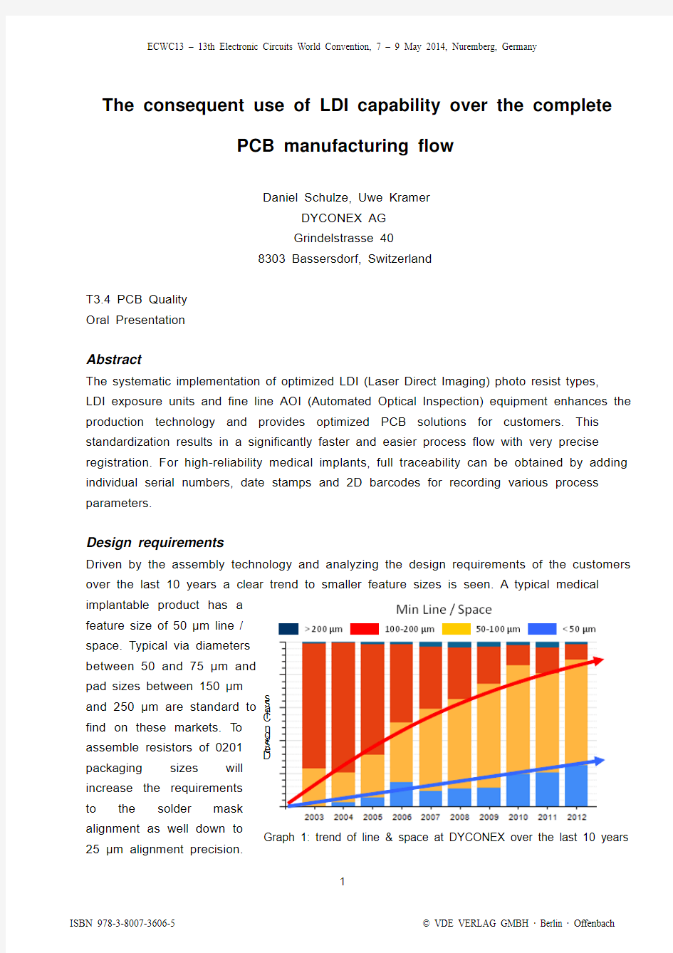
Driven by the assembly technology and analyzing the design requirements of the customers over the last 10 years a clear trend to smaller feature sizes is seen. A typical medical implantable product has a
feature size of 50 μm line /
space. Typical via diameters
between 50 and 75 μm and
pad sizes between 150 μm and 250 μm are standard to
find on these markets. To
assemble resistors of 0201
packaging
sizes will increase the requirements to the solder mask
alignment as well down to
25 μm alignment precision.
During the quotation phase a detailed design rule check (DRC) has to be done to analyze customers design requirements. Dependent on these requirements like annular ring, layer to layer accuracy or solder mask to artwork accuracy the right registration systems have to be chosen to define the most cost effective and precise manufacturing flow.
The graph below shows that the corresponding alignment accuracies are dependant on the customer design and finally used registration concept within the PCB manufacturing.
Graph 3: registration concept dependant on customer design class using the annular ring as example
Graph 2: typical misalignment failure modes Registration Systems
Laser via LDI Artwork Solder mask
Mechanical via LDI Artwork Solder mask
Plasma via LDI Artwork Solder mask
average compensation
step & repeat compensation
average compensation
individual compensation
individual compensation
individual compensation
individual compensation
average compensation
average compensation
average compensation
average compensation
Equipment requirements
The challenge for PCB manufacturers is to constantly implement new manufacturing technologies to satisfy the customers growing demand in PCB complexity, cost efficiency and shorter delivery cycle times. In addition these requirements from the customers have to be linked to profitability of the supplier. One
of the trends which has been observed
during the last years is the direct imaging
technology. The growing market for direct
imaging tools reflects the increasing
variety of DI (Direct Imaging)
technologies and vendors. Specialized
systems for different requirements are available. There are entry level systems,
tools with double stage loading for faster throughput, high resolution systems and systems which cope with imaging of solder mask. All these systems offer a great variety of advantages over conventional film exposure which will be described in detail in the next chapters. Before starting with DI technology in production one needs to think about the specifications for the equipment. What should the tools be used for? What is the conversion strategy from film imaging to DI? Are there restrictions from customers which need to be addressed? Should and can the equipment operate in automated mode without operator support? What advantages in detail are of interest for the production environment?
Due to the demands of customers the requirements on DI systems are well defined. A film plotter has a resolution of 2.5 μm pixel size in comparison to a modern LDI with coherent light and 1 μm pixel size. Therefore LDI systems can offer resolutions higher than 20 μm line and space. Further requirements of the LDI equipment are registration performance better than 10 μm and programmable compensation schemes to include individual compensation together with step & repeat compensation. Furthermore, the systems need to be able to expose solder masks within a competitive process time. Customers are asking for full traceability during PCB manufacturing. Therefore, implementation of individual serial numbers, bar codes or date stamps during imaging is an important feature.
After having defined all these prerequisites the process environment needs to be evaluated for matching the DI properties. Contrary to standard film foil exposure units most LDI systems use only one wavelength. When
starting with LDI processing in
production photo resists are typically
not optimized for direct imaging. This
means they either require longer
exposure times compared to film
foil Graph 4: film exposure and LDI exposure equipment
Graph 5: conventional exposure vs. LDI exposure
exposure or they are not suitable at all for DI. Even if the standard photo resist can be exposed with DI the change to LDI optimized resists should be taken into account. Today there is a very big variety of optimized DI resists available on the market. After implementing these resists the cycle time for artwork imaging in comparison to film imaging is significantly reduced.
Compared to photo resists conventional solder mask exposure requires much higher exposure energy; up to 800mJ/cm2. When establishing direct imaging processes in manufacturing this fact needs to be taken into account. Depending on other requirements the DI capacity needs to be calculated to be sufficient for conventional solder mask exposure. Optimized direct imaging tools are available on the market which combines both the advantages of direct imaging and the high exposure energy. The other option is to qualify new solder mask materials which are optimized for DI. As mentioned above the need for direct imaging of solder masks is usually given on very thin flex products. However, only a limited number of flexible solder masks are available. These solder masks can be exposed with less than 100mJ/cm2. Since medical customers can not change solder mask during the life cycle of a certified product a qualification of a solder mask for direct imaging is a long-term and strategic decision. Therefore at DYCONEX we have qualified two types of flex solder mask for direct imaging. When applying the solder mask optimized for direct imaging an exposure cycle time of less than 90 seconds per panel is achieved. In comparison to LDI solder mask, conventional solder mask exposure takes 6 times longer.
Registration Concepts
Substrate materials are changing in size during the various manufacturing steps. For example plating, desmearing or any process steps where heat is applied. Therefore a start compensation value is given to the substrates to accommodate for the shrinkage or expansion. Changing the single step artwork exposure to LDI has an influence on the rest of the manufacturing process steps. Conventional film foil exposure with just one single compensation value for the entire manufacturing lot as opposed to single panel compensation value to each individual panel using LDI. Thus the complete registration chain from the beginning of the first drilling step through to the artwork and solder mask exposure and ending up with the final routing has to be reviewed.
One of the conventional registration concepts is to build sequential products and align layer to layer referring directly to the inner layer structure. A newer registration system uses x-ray drilling to reference to one or more inner layers at simultaneously. Changing from conventional multilayer registration concept to LDI offers several advantages: less process steps, faster through put time and higher alignment precision.
The lower number of process steps in the work flow for LDI registration system is seen in Graph 6. For the conventional registration the reference system needs to be protected with
4
stickers prior to plating. The punching of the reference system needs to be done. After that the compensation needs to be measured and the films need to be plotted. During exposure the film needs to be aligned to the panel and for good imaging performance vacuum needs to be applied. If required additional sets of films need to be plotted where compensation deviations within the work order occur. The exposure process itself is typically performed simultaneously on front and back of the panel. The overall process time including the supporting processes is 5 - 10 minutes per panel.
For the LDI registration process the reference system can be drilled and does not need to be protected. No film needs to be plotted and the individual compensation does not need to be measured in advance. The exposure of front and back is done sequentially. The overall process time including application of resist is less than 2 minutes per panel.
Graph 6: comparison between conventional registration and LDI registration system
Compensation concepts
Basically within the film exposure process only an average compensation for the entire lot of multiple panels is possible. Depending on the LDI equipment used a variety of different compensation schemes can be applied:
? average compensation
? individual panel compensation
? step & repeat compensation (sub panel scaling)
Step & repeat scaling can help when high
compensation offsets are present within a work
order. Individual compensation is not feasible
due to the following processes where only
average compensation, like final mechanical
routing or screen printing has been applied.
The most accurate and at the same time most
complex scaling concept is the step and repeat
registration and compensation.
Comparisons between different compensation
schemes show the performance improvements.
Very thin flex material tends to non linear distortions which occur through the entire manufacturing process. These distortions can not be compensated completely. All remaining distortions which can not be corrected are reflected in loss of annular ring and misregistration. Together with the increasing complexity as mentioned in the beginning of this paper the annular ring requirements are also increasing. Today standard alignment requirements are 25 μm for both artwork and solder mask. Typically thin flex material distortions within a workorder can be higher than 300 ppm. This can result, depending on panel size in more than 50 μm loss in annular ring.
When film foil exposure is applied no kind of deviation can be corrected. When using individual panel scaling the panel to panel variation can be compensated. This reduces the
amount of annular ring failures by a factor of two. The impact of the non linear distortions can Graph 8: material distortion within one single panel
Graph 7: material distortion within a work order of multiple production panels
be reduced when step & repeat registration is applied. Measurements on 25 μm flex material show that the registration within one workorder is improved again by a factor of two. The conclusion of this is that only DI systems can guarantee the high yields to satisfy increasing demands on high density PCB’s.
When individual or step & repeat compensation is applied the same compensation methods should be applied to the following process steps. As an example the artwork and solder mask on a 25 μm thin flex panel is imaged using step & repeat compensation. This results in 25 μm registration accuracy. Nevertheless the distortions within a panel are higher than this. Therefore the final mechanical routing also has to be done with step & repeat compensation. Otherwise positioning failure of the PCB structures relative to the routing contour will occur. In other words, the full potential of individual or step & repeat compensation needs to be considered for the entire process chain.
Individual and step & repeat compensations in artwork imaging are well established in the PCB industry already. Same holds true for laser processing. Last but not least the solder mask imaging is the process which also needs to be converted to direct imaging.
average compensation = x panel individual compensation = 1 panel
S&R compensation = 1/x panel
average compensation individual compensation
S&R compensation Graph 10: registration performance depend on used registration concept
Traceability Information
As mentioned above most customers ask for traceability of their products through the entire manufacturing process. Traceability means a unique numbering of the manufacturing lot, panel, delivery panel and print at least. This can mean bar codes and date stamp of customer specific counters. Since for DI process no film needs to be plotted, these features can be implemented directly during exposure. The individual features are etched in copper. The same can be done when solder mask is exposed with direct imaging. On some products a legend print is included. Even here the individual serial number can be exposed. At DYCONEX all artwork exposures enable individual serial numbers for full traceability.
Graph 11: Traceability information with LDI exposure and copper etched
Conclusion
To achieve higher yields and faster trough-put times a change from conventional manufacturing technologies like film exposure to advanced manufacturing processes like laser direct imaging is necessary for high-end, high-reliability flexible PCB’s in the medical, avionics or semiconductor market. To use LDI exposure in PCB manufacturing requires several equipment updates. Changing the photo chemistry lines and implementing new photo resists or reference systems are just some examples. Following this path results in a new spectrum of smaller and more miniaturized PCB’s with the advantage of better alignment registration, higher accuracy, faster through put time and a better traceability.
Manufacturer ID
Lot Number
Panel Number
Prin t Position Number
Date Code
Customer Article Number 2D Barcode
copper etched
Biography
Mr. Daniel Schulze studied at the Technical University of Dresden and has a diploma degree in Electrical Engineering. During his diploma thesis and an internship at the Georgia Tech Packaging Research Center he got involved with the work on optical waveguides embedded in PCB’s. In 2005 he started to work as Product Engineer at DYCONEX. Since 2008 he is Engineering Manager at DYCONEX and responsible for the product development of medical imaging PCB’s, hearing aids and cochlear implants, industrial and HF products.
Mr. Uwe Kramer studied at the University of Halle/Wittenberg and the Technical University Dresden. He holds a diploma degree in physics. He is specialized in semiconductor and metal physics. The diploma thesis was done in collaboration with Advanced Micro Devises and Fraunhofer Institute for Mechanics of Materials. Thesis of diploma was three dimensional reconstruction and analysis of grain structure by using fine beam techniques. Mr. Kramer joined DYCONEX in 2008 as process engineer. Since 2013 he is manager of the process module artwork and senior process engineer.
空中成像技术原理
360度空中悬浮成像 产品简介 悬浮成像又称空中悬浮成像、360度幻影成像、360度悬浮成像等。空中悬浮成像系统是一项新颖多媒体演示系统,具有三维空间成像的功能,空中悬浮成像是近年来在国际上兴起的一种新型展示技术,该技术可以使立体影像不借助任何屏幕或介质而直接悬浮在设备外的自由空间,观众可以不佩戴任何辅助工具(如立体眼镜、VR头盔等)直接用裸眼观看立体影像,由于影像的清晰度及色彩还真度高,立体感强,因此非常逼真,可以给观众以新奇、玄妙的视觉冲击,激发观众探究欲,并可以起到聚集现场人气、加深参观者印象、提高被展示物知名度的作用。 技术原理 360度幻影成像产品展示系统是以宽银幕的环境、场景模型和灯光的传换,给人以视觉上的冲击。观众可从。由柜体,分光镜,射灯,视频播放设备组成,基于分光镜成像原理,通过对产品实拍构建三维模型的特殊处理,然后把拍摄的产品影像或产品三维模型影像叠加进场景中,构成了动静结合的产品展示系统。最终向观众展示融入实景的产品模型幻影成像效果。 成像原理 半透半反玻璃:就是在玻璃表面通过真空磁控溅射镀膜工艺镀制纳米级的氧化物介质膜层,使玻璃保持较高的透过率(50%—70%)的同时也具有高的反射率(镜面外观)。膜层主要成分是二氧化钛(TiO2)。该玻璃表面硬度高,还具有一定的自洁、防水雾、光催化活性等特性。与普通玻璃相比,半透半反玻璃的光线反射率和直射率相等,因此呈现的虚像较为清晰,所以在幻影成像系统中选用此类玻璃作为成像的介质。 视频发射器将光信号发射到这个锥体中的特殊棱镜上,汇集到一起后形成具有真实维
度空间的立体影像。通过表面镜射和反射,观众能从锥形空间里看到自由飘浮的影像和图形。 360度悬浮成像系统由主体模型场景、造型灯光系统、光学成像系统、影视播放系统、计算机多媒体系统、音响系统及控制系统等组成。 实物示例:
PCB制作过程中激光直接成像的三种方式
PCB制作过程中激光直接成像的三种方式 激光直接成像让pcb制作工艺过程简化了至少60%,而传统的底片图片转移却需要十几个步骤。那么PCB制作过程中激光直接成像都有哪些方式呢?全世界的pcb制作商所配备的LDI设备都属于UV光的LDI,按其工艺可以具体分为三种: 1)光致抗蚀剂的激光直接成像。这一类型是指对涂覆有专用光致抗蚀剂的在制板进行激光直接成像。在制板上要完成导电图形基于如下三个步骤: 第一步:利于LDI在激光直接在制板上的专用光致抗蚀剂进行感光。激光感光是由cad图形数据或计算机已存储的图形数据进行控制激光扫描的,而专业光致抗蚀剂的光敏性要比传统的光致抗蚀剂光敏要强得多(约10倍)来进行激光扫描,才能取得高的PCB图形转移的生产率。
第二步:化学显影。专用光致抗蚀剂仍采用传统的弱碱性碳酸钠溶液进行显影。 第三步:化学蚀刻。由于专用的光致抗蚀剂是属于耐酸性(或则耐酸性强于耐碱性)的,因此要采用酸性氯化铜蚀刻溶液等来进行蚀刻。 2)pcb制作采用化学镀锡的激光直接成像。 在制板上化学镀锡的激光直接成像(LDI),某些文献又称为激光直接刻板。这一类型是指在制板上利用化学方法镀上一层很薄的抗蚀层锡,然后利用激光蚀刻去不需抗蚀刻、保护的锡层及底下的部分厚度(3μm~5μm)的铜箔,然后进行化学蚀刻。由于锡层在0.5μm~1.0μm厚度)是抗碱不耐酸的。 3)以覆铜箔的在制板上的激光直接成像,这一类型是指仅在覆铜箔在制板上的激光直接成像。他不需要对在制板进行任何涂覆抗蚀保护层,而是直接利用激光蚀刻去不需要的铜
箔,但是为了损伤介质厚度,往往还留下3μm~5μm厚度的铜箔,然后进行严格控制的快速化学蚀刻而出去留下的铜箔厚度。因此在制板上的铜导体图形的铜厚度将会变薄些。这具体问题具体分析。 综上所述我们了解到了PCB生产制作过程中使用的激光直接成像的类型方式,工艺在于精益求精,不断实践和优化提升。深圳金瑞欣特种电路是专业的电路板打样和中小批量生产厂家,主营2-30层高多层板,、高频板、厚铜板、Hdi板等。更多详情可以咨询金瑞欣特种电路官网。
线路板制作工艺流程
线路板制作工艺流程(一) 作者:pcbinf 发表时间:2009-10-15 前言 在印制电路板制造过程中,涉及到诸多方面的工艺工作,从工艺审查到生产到最终检验,都必须考虑到工艺质量和生产质量的监测和控制。为此,将曾通过生产实践所获得的点滴经验提供给同行,仅供参考。 第一章工艺审查和准备 工艺审查是针对设计所提供的原始资料,根据有关的"设计规范"及有关标准,结合生产实际,对设计部位所提供的制造印制电路板有关设计资料进行工艺性审查。工艺审查的要点有以下几个方面: 1,设计资料是否完整(包括:软盘、执行的技术标准等); 2,调出软盘资料,进行工艺性检查,其中应包括电路图形、阻焊图形、钻孔图形、数字图形、电测图形及有关的设计资料等; 3,对工艺要求是否可行、可制造、可电测、可维护等。 第二节工艺准备 工艺准备是在根据设计的有关技术资料的基础上,进行生产前的工艺准备。工艺应按照工艺程序进行科学的编制,其主要内容应括以下几个方面:
1,在制定工艺程序,要合理、要准确、易懂可行; 2,在首道工序中,应注明底片的正反面、焊接面及元件面、并且进行编号或标志; 3,在钻孔工序中,应注明孔径类型、孔径大小、孔径数量; 4,在进行孔化时,要注明对沉铜层的技术要求及背光检测或测定; 5,孔后进行电镀时,要注明初始电流大小及回原正常电流大小的工艺方法; 6,在图形转移时,要注明底片的药膜面与光致抗蚀膜的正确接触及曝光条件的测试条件确定后,再进行曝光; 7,曝光后的半成品要放置一定的时间再去进行显影; 8,图形电镀加厚时,要严格的对表面露铜部位进行清洁和检查;镀铜厚度及其它工艺参数如电流密度、槽液温度等; 9,进行电镀抗蚀金属-锡铅合金时,要注明镀层厚度; 10,蚀刻时要进行首件试验,条件确定后再进行蚀刻,蚀刻后必须中和处理; 11,在进行多层板生产过程中,要注意内层图形的检查或AOI检查,合格后再转入下道工序; 12,在进行层压时,应注明工艺条件; 13,有插头镀金要求的应注明镀层厚度和镀覆部位; 14,如进行热风整平时,要注明工艺参数及镀层退除应注意的事项;
PCB全制作流程中的激光直接成像技术应用
Graph 1: trend of line & space at DYCONEX over the last 10 years The consequent use of LDI capability over the complete PCB manufacturing flow Daniel Schulze, Uwe Kramer DYCONEX AG Grindelstrasse 40 8303 Bassersdorf, Switzerland T3.4 PCB Quality Oral Presentation Abstract The systematic implementation of optimized LDI (Laser Direct Imaging) photo resist types, LDI exposure units and fine line AOI (Automated Optical Inspection) equipment enhances the production technology and provides optimized PCB solutions for customers. This standardization results in a significantly faster and easier process flow with very precise registration. For high-reliability medical implants, full traceability can be obtained by adding individual serial numbers, date stamps and 2D barcodes for recording various process parameters. Design requirements Driven by the assembly technology and analyzing the design requirements of the customers over the last 10 years a clear trend to smaller feature sizes is seen. A typical medical implantable product has a feature size of 50 μm line / space. Typical via diameters between 50 and 75 μm and pad sizes between 150 μm and 250 μm are standard to find on these markets. To assemble resistors of 0201 packaging sizes will increase the requirements to the solder mask alignment as well down to 25 μm alignment precision.
电路板制作流程稿
电路板制作流程(稿) 李仕兵日期:2003-2-13 电路板制作是一门专业的学问,它涉及了很多方面的知识,如电学、磁学、美学、机械学、空间想象思维等多方面的知识,还需要了解市场行情,电子科技发展等。可以说,一块简单或要求不高的电路板,只要学会了制作工具(如PROTEL9)就可以制作。但一块好的要求高的电路板,你就要从原理图优化设计,到PCB的合理布置都要经过精心的考虑。电路板的绘制要有讲究,不能随便放置元件,在考虑电气性能通过良好的基础上,要考虑到元件的大小、高低搭配一致,做到有层次感。电路板上属于同一功能块的元件应尽量放在一起,发热量大的元件要用较宽的敷铜区把元件底部与元件外的空区域连接在一起,利用了铜的良导热性把热量导走到外面的大面积处,增大散热面积,便于散热。好的板需要考虑线路简洁,电路通畅,电磁兼容,抗干扰能力强,是高频要上得去,元件在电路板上密度要大致均匀,高低适当,尽量美观大方。 拿到一幅电路图,首先看清楚电路的原理、功能,控制和被控对象,理清电路的逻辑。制作电路板,尽可能做到“一次定型”,避免浪费现象。 绘制电路板的过程步骤,一般如下: 位按键用RST或RESET等。也可使用自动标注,把各个元件标注不同的序号,但一般都是自动标注带问号 (?)的,如R?,D?等,这样使个类元件名称分开,方便查阅和检查。 2?电气规则检查。简单的原理图出错几率比较小,复杂的电路原理图由于所用元件较多,网络节点较多,网络繁复,这样人为检查就容易漏掉一些错误,如网络标号多一字母或少一字母,有时又只写了一个网络标号,或者有两个元件用同一个名的,这些错误使用电气规则检查一般都能检查岀来。还有一些电路原理上的错误,可以在后来绘制PCB时,通过仔细的分析发现。 3?封装。给元件一个合适的外形形状,便于使实物与所绘制的PCB板对应。一个元件可以使用不同的 封装,一个封装也可用于不同的元件。适当的封装应该是和元件刚好配合,这样就需要在元件封装前了解 实物的大小,管脚间距,外形尺寸。常用封装如:
激光共聚焦显微镜与普通显微镜成像原理及区别
激光扫描共聚焦显微镜采用激光作为光源, 有效地除去了非聚焦平面的信息, 提高了微观形貌的清晰度和分辨率。其与计算机软件结合可以实现深度方向的光学切片观察, 再将这些扫描得到的信息通过软件算法以及叠加和重组, 可以获得材料的微观三维形貌, 因此激光共聚焦显微镜具有快速、无损、制样简单等优点。那么激光共聚焦显微镜的原理又是怎样的呢? 它采用激光点光源照射样品, 从发射器发出的光经过光路后在聚焦平面上形成一个大小分明的光点,它沿着原照射光路到达分光镜并且该点发出的光被物镜收集,分光镜将收集来的光直接反馈给探测器。光点通过前方探测器设有的探测针孔等一系列的透镜, 最终同时聚焦于探测针孔, 这样来自聚焦平面的光可以会聚在探测孔之内, 而来自聚焦平面上方或下方的散射光都被挡在探测孔之外而不能成像, 从而提高了焦平面的分辨率。激光共聚焦显微镜逐点扫描样品, 探测针孔后的光电倍增管也逐点获得对应光点的共聚焦图像, 转为数字信号传输到计算机上, 最终在屏幕上聚合成清晰的整个焦平面的共聚焦图像。转为数字信号传输到计算机上, 最终在屏幕上聚合成清晰的整个焦平面的共聚焦图像。此外激光共聚焦显微镜还可以对样品进行逐层光学切片扫描, 得到高度方向每一层的图像信息, 传回计算机软件叠加处理后可以得到三维形貌图。它成像清晰、精确、最大的优点在于能对材料进行深层形貌的观察。可以对样品进行断层扫描观察和成像, 进行无损观察和三维形貌分析。 激光共聚焦显微镜可用来观察样品表面亚微米级别的三维轮廓形貌, 也可以测量多种微几何尺寸, 像晶粒度、体积、膜深、膜厚、深度、长宽、线粗糙度、面粗糙度等。激光共
聚焦相比于其他测量手段有其独特的优势, 它提高了图片的清晰度, 有很好的景深, 提高了分辨率, 可以进行无接触的三维轮廓测试。在金属材料研发方面还经常用到光学显微镜和扫描电子显微镜。光学显微镜是一种二维的形态学工具, 有效分辨率较低, 分辨率的景深较小, 也不能观察纵向方向的三维形态。而扫描电镜在样品的制备方面比较复杂, 有时还会引起样品的破坏, 对于扫描的面积和材料的表面高度都有所限制, 同时它也不能测量面积、体积、深度等信息。在钢铁材料的生产和开发过程中, 众多的环节需要关注表面形貌, 采用激光共聚焦显微镜技术进行相应检测, 不仅可以获得媲美SEM的显微图像, 同时还能够进行快速、无损测量, 加之其较低的引入和维护成本,更符合目前行业成本控制的需求。本文将举例说明激光共聚焦显微镜在金属研究领域的典型应用。 激光共聚焦显微镜由于其优于光学显微镜的清晰度和分辨率, 使其在金相组织观察方面有独特的优势。试验样品为海洋平台用钢, 将样品进行磨制、抛光处理, 并用腐蚀溶液腐蚀, 要求观察并测量基体上粒状贝氏体的形态和尺寸。相比于普通光学显微镜, 激光共聚焦显微镜清晰度好, 分辨率高。激光作为光源, 它的单色性非常好, 光束的波长相同, 从根本上消除了色差。共聚焦显微镜中在物镜的焦平面上放置了一个带有针孔的挡板, 将焦平面以外的杂散光挡住, 从而消除了球差。同时激光共聚焦显微镜采取的点扫描技术和计算机采集和处理信号也进一步提高了图像的清晰度。
PCB板制造工艺流程
PCB板制造工艺流程 PCB板的分类 1、按层数分:①单面板②双面板③多层板 2、按镀层工艺分:①热风整平板②化学沉金板③全板镀金板④热风整平+金手指 3、⑤ 化学沉金+金手指4、⑥全板镀金+金手指5、⑦沉锡⑧沉银⑨OSP板 各种工艺多层板流程 ㈠热风整平多层板流程:开料——内层图像转移:(内层磨板、内层贴膜、菲林对位、曝光、显影、蚀刻、褪膜)——AOI——棕化——层压——钻孔——沉铜——板镀——外层图像转移:(外层磨板、外层贴膜、菲林对位、曝光、显影、图镀、褪膜、蚀刻、褪锡)——丝印阻焊油墨——阻焊图像转移:(菲林对位、曝光、显影)——丝印字符——热风整平——铣外形——电测——终检——真空包装 ㈡热风整平+金手指多层板流程:开料——内层图像转移:(内层磨板、内层贴膜、菲林对位、曝光、显影、蚀刻、褪膜)——AOI——棕化——层压——钻孔——沉铜——板镀——外层图像转移:(外层磨板、外层贴膜、菲林对位、曝光、显影、图镀、褪膜、蚀刻、褪锡)——丝印阻焊油墨——阻焊图像转移:(菲林对位、曝光、显影)——镀金手指——丝印字符——热风整平——铣外形——金手指倒角——电测——终检——真空包装 ㈢化学沉金多层板流程:开料——内层图像转移:(内层磨板、内层贴膜、菲林对位、曝光、显影、蚀刻、褪膜)——AOI——棕化——层压——钻孔——沉铜——板镀——外层图像转移:(外层磨板、外层贴膜、菲林对位、曝光、显影、图镀、褪膜、蚀刻、褪锡)——丝印阻焊油墨——阻焊图像转移:(菲林对位、曝光、显影)——化学沉金——丝印字符——铣外形——电测——终检——真空包装 ㈣全板镀金板多层板流程:开料——内层图像转移:(内层磨板、内层贴膜、菲林对位、曝光、显影、蚀刻、褪膜)——AOI——棕化——层压——钻孔——沉铜——板镀——外层图像转移:(外层磨板、外层贴膜、菲林对位、曝光、显影、图镀镍金、褪膜、蚀刻、褪锡)——丝印阻焊油墨——阻焊图像转移:(菲林对位、曝光、显影)——丝印字符——铣外形——电测——终检——真空包装(全板镀金板外层线路不补偿) ㈤全板镀金+金手指多层板流程:开料——内层图像转移:(内层磨板、内层贴膜、菲林对位、曝光、显影、蚀刻、褪膜)——AOI——棕化——层压——钻孔——沉铜——板镀——外光成像①(外层磨板、外层贴膜、菲林对位、曝光、显影)——图形电镀铜——镀镍金——外光成像②(W—250干膜)——镀金手指——褪膜——蚀刻——丝印阻焊油墨——阻焊图像转移:(菲林对位、曝光、显影)——镀金手指——丝印字符——铣外形——金手指倒角——电测——终检——真空包装 ㈥化学沉金+金手指多层板流程:开料——内层图像转移:(内层磨板、内层贴膜、菲林对位、曝光、显影、蚀刻、褪膜)——AOI——棕化——层压——钻孔——沉铜——板镀——外层图像转移:(外层磨板、外层贴膜、菲林对位、曝光、显影、图镀、褪膜、蚀刻、褪锡)——化学沉金——丝印字符——外光成像②(交货面积>1平方米)/贴蓝胶带(交货面积≤1平方米)——镀金手指——铣外形——金手指倒角——电测——终检——真空包装 ㈦单面板流程(热风整平为例):开料——钻孔——外层图像转移:(外层磨板、外层贴膜、菲林对位、曝光、显影、图镀、褪膜、蚀刻、褪锡)——AOI——丝印阻焊油墨——阻焊图像转移:(菲林对位、曝光、显影)——丝印字符——热风整平——铣外形——电测——终检——真空包装(注:①因没有金属化孔,所以没有电测与沉铜板镀②外层线路菲林除全板镀金板用正片菲林外,其它都用负片) ㈧双面板流程(热风整平为例):开料——钻孔——沉铜——板镀——外层图像转移:(外层磨板、外层贴膜、菲林对位、曝光、显影、图镀、褪膜、蚀刻、褪锡)——丝印阻焊油墨——阻焊图像转移:(菲林对位、曝光、显影)——丝印字符——热风整平——铣外形——
激光雷达与激光成像雷达
激光雷达与激光成像雷达 一、激光雷达与激光成像雷达 一、激光雷达与激光成像雷达 人通过感觉器官感知,认识外部世界的一切。用耳朵听音乐、话音、机器的轰隆声、钟声、铃声等一切通过声音传递的信息;用手感觉温度、物体的硬软以及物质的存在;用眼睛观察外部世界的形状、颜色、运动状态、速度、位置、识别物体的种类等等。人的眼睛之所以可以看见外部世界,是因为太阳光谱中的可见光照射在物体上反射的结果。那么除了“可见光谱”之外还存在别的“不可见的光谱”吗?事实上,广义的光谱按频段的不同,有大家所熟悉的电磁波、远红外、近红外、可见光、紫外光谱,而可见光谱区中,红色的光波长最长,紫色的波长最短。而且人们已经发现不同的物质辐射不同的谱线,在特定的条件下还可以只辐射某一单一波长的谱线,当其人们发现不可见光谱区中的单一的光谱谱线具有可贵的特性的时候,就力图去产生、开发、利用这种单一光谱谱线,由此产生了激光及用于不同场合的激光系统。 视觉引发人们的形象思维,眼睛从外界事物所获取的信息量大,直接而快速,是其他感觉器官所不能代替的,这也就是古人所说的“眼见为实”的深切内涵。正是因为这个道理,人们不愿受限于“可见光”的可见,而想去探求自然光条件下所看不见的东西,如想在漆黑的夜晚,去观察外部世界,就开发出了“夜视仪”。被动“红外热成像仪”也不是依赖于可见光的反射特性去观察变幻莫测的外部世界的,而是依赖于物体本身的热辐射,无论白天或黑夜都可以用以观察人类世界的一切,而且已经是超视距的。目前最新的热成像仪,1ms内热敏成像。红外成像高速测温用来检测来复枪,其射出的弹头在弹道上飞行速度为840m/s,弹头距枪口0.914 4m处的热成像还能分辨出弹头上不同部位摩擦热的温差。 遥感仪则可以依据物体本身的辐射谱线,包括电磁波段与红外光区,远距离成像,把肉眼原本看不见的自然变化,转化为可见,以照片的形式或屏幕显示的图像,甚至动态图像的形式展现出来,这就是当今人们感兴趣的可视化技术。人们力图从各个领域做这方面的研究和开发应用。 通过眼睛人们能够确定方向——定位,作为控制手的动作的依据,当然这是受限于“视距”之内的,通过望远镜可以延伸视距;但是“定位”的精度达不到人们通用目的需要,所谓“差之毫厘,失之千里”。雷达满足了远距离定位和精度的要求,雷达源于英文Radio Detection And Ranging的缩写RADAR,于1935年问世。 当其“激光”这种波长处于红外光谱波段的“激光光源”被研究出来之后,人们自然想到利用微米波段(红外光谱波段)的光波作为信息的载体去探测、获取其他手段难于探测、观测到的目标的信息。激光雷达研制成功后,相继激光成像雷达应运而生。激光雷达的英文名字“LADAR”是Laser Detection And Ranging的缩写。激光雷达的研究是从目标探测和测距入手的,早期(1962~1976年)的研究系统被称为光雷达(Optical RADAR),并命名为LIDAR(Light Detection And Ranging)。可以说军事应用对测量系统精确度的要求日
线路板生产工艺流程
线路板生产流程(一) 多种不同工艺的PCB 流程简介 *单面板工艺流程 下料磨边T钻孔T外层图形T(全板镀金)7蚀刻T检验T丝印阻焊T (热风整平)7丝印 字符T外形加工T测试T检验 *双面板喷锡板工艺流程 下料磨边7钻孔7沉铜加厚7外层图形7镀锡、蚀刻退锡7二次钻孔7检验7丝印阻焊7镀金插头7热风整平7丝印字符7外形加工7测试7检验 *双面板镀镍金工艺流程 下料磨边7钻孔7沉铜加厚7外层图形7镀镍、金去膜蚀刻7二次钻孔7检验7丝印阻焊7 丝印字符7外形加工7测试7检验 *多层板喷锡板工艺流程下料磨边7钻定位孔7内层图形7内层蚀刻7检验7黑化7层压7钻孔7沉铜加厚7外层图形7镀锡、蚀刻退锡7二次钻孔7检验7丝印阻焊7镀金插头7热风整平7丝印字符7外形加工7测试7检验 *多层板镀镍金工艺流程下料磨边7钻定位孔7内层图形7内层蚀刻7检验7黑化7层压7钻孔7沉铜加厚7外层图形7镀金、去膜蚀刻7二次钻孔7检验7丝印阻焊7丝印字符7外形加工7测试7检验 *多层板沉镍金板工艺流程下料磨边7钻定位孔7内层图形7内层蚀刻7检验7黑化7层压7钻孔7沉铜加厚7外层图形7镀锡、蚀刻退锡7二次钻孔7检验7丝印阻焊7化学沉镍金7丝印字符7外形加工7 测试7检验 一步一步教你手工制作PCB 制作PCB 设备与器材准备 (1) DM-2100B 型快速制板机1 台 (2) 快速腐蚀机1 台 (3) 热转印纸若干 (4) 覆铜板1 张 (5) 三氯化铁若干 (6) 激光打印机1 台 (7) PC机1台
(8) 微型电钻1个 (1) DM-2100B型快速制板机 DM 一2100B型快速制板机是用来将打印在热转印纸上的印制电路图转印到覆铜板上的设备, 1) 【电源】启动键一按下并保持两秒钟左右,电源将自动启动。 2) 【加热】控制键一当胶辊温度在100C以上时,按下该键可以停止加热,工作状态显示 为闪动的“ C”。再次按下该键,将继续进行加热,工作状态显示为当前温度;按下此键后, 待胶辊温度降至100C以下,机器将自动关闭电源;胶辊温度在100C以内时,按下此键, 电源将立即关闭。 3) 【转速】设定键一按下该键将显示电机转速比,其值为30(0.8转/分)?80(2.5转份)。按 下该键的同时再按下”上"或"下"键,可设定转印速度。 4) 【温度】设定键一显示器在正常状态下显示转印温度,按下此键将显示所设定温度值。 最高设定温度为180~C,最低设定温度为100C ;按下此键的同时再按下”上"或"下"键,可设定温度。 5) "上"和"下"换向键一开机时系统默认为退出状态,制板过程中,若需改变转向,可直接按此键。 (2) 快速腐蚀机 快速腐蚀机是用来快速腐蚀印制板的。 其基本原理是,利用抗腐蚀小型潜水泵使三氯化铁溶液进行循环,被腐蚀的印制版就处 在流动的腐蚀溶液中。为了提高腐蚀速度,可加热腐蚀溶液的温度。 (3) 热转印纸 热转印纸是经过特殊处理的、通过高分子技术在它的表面覆盖了数层特殊材料的专用纸,具有耐高温不粘连的特性? (4) 微型电钻 微型电钻是用来对腐蚀好的印制电路板进行钻孔的。 4 ?实训步骤与报告 (1). PCB图的打印方法 启动Protel 98 一打开设计的PCB图-单击菜单栏中的File-Setup Printer 一获得Printer Setup 对话框.
主动成像激光雷达
第37卷,增刊 红外与激光工程 2008年9月 V ol.37 Supplement Infrared and Laser Engineering Sep. 2008 收稿日期:2008-09-22 作者简介:杨鹏(1981-),男,河南南阳人,博士研究生,主要从事光电位移测量光电研究。Email:rocyangpeng@https://www.360docs.net/doc/47354078.html, 导师简介:艾华(1961-),男,吉林长春人,研究员,博导,主要从事光电位移测量、光电测控研究。Email:aih ◎https://www.360docs.net/doc/47354078.html, 主动成像激光雷达 杨 鹏1,2,王宇志1,2,李 琳1,2,艾 华1 (1.中国科学院长春光学精密机械与物理研究所, 吉林 长春 130033; 2.中国科学院研究生院, 北京 100039) 摘要:主动成像激光雷达由系统本身提供照明,不必再依赖太阳角,可全天候工作,具有远距离、高分辨率、三维成像能力。特别是具有目标探测、识别和辨识等方面的超强能力,战场上在预警、信息获取、目标监视和侦查方面有很重要的应用。介绍了两种不同体制主动成像激光雷达:一种是采用相干成像合成孔径红外激光雷达,另一种是采用孔径平面散斑强度信息成像激光雷达。阐述了两种不同体制主动成像激光雷达的原理、特点和研究现状,并对其关键技术和应用前景进行了简要的分析。 关键词:激光雷达; 合成孔径; 散斑成像; 相干探测 中图分类号:TN958.98 文献标识码:A 文章编号:1007-2276(2008)增(激光探测)-0115-05 Active imaging ladar YANG Peng 1,2 ,WANG Yu-zhi 1,2, LI Lin 1,2 , AI Hua 1 (1. Changchun Institute of Optics, Fine Mechanics and Physics, Chinese Academy of sciences, Changchun 130033, China ; (2. Graduate School of the Chinese Academy of sciences, Beijing 100039, China ) Abstract: Active imaging ladar, because they provide their own illumination, are capable of operating 24 hours a day and are not dependent upon the angle of the sun. They can provide ultra-high resolution and three-dimensional imaging at long range. These capabilities would be promising in target detection and remote sensing and mapping. These capabilities would improve Battlefield Awareness (BA) and provide persistent Intelligence, Surveillance, and Reconnaissance (ISR) to perform target detection, recognition, and identification. This paper discusses two different approaches to active optical imaging. One is a coherent approach that uses synthetic aperture techniques with infrared laser radar, and another approach uses only the intensity of the speckle pattern in the aperture plane. Two different approaches to active optical imaging are introduced. The principle, advantage and progress of these two ladar systems are described. The key techniques and application prospect of them are also briefly discussed. Key words: Ladar; Synthetic aperture; Speckle imaging; Coherent detection 0 引 言 主动成像激光雷达工作在光学波段,其工作波长 远小于普通微波雷达,因此可以获得高分辨率的目标图像,这些图像看起来更自然、更容易理解,因此,其在军事侦察和遥感测绘等方面具有广阔的应用前景。主要介绍了两种不同体制的成像激光雷达,都具
pcb制作流程
pcb制作流程: 根据电路功能需要设计原理图。原理图的设计主要是依据各元器件的电气性能根据需要进行合理的搭建,通过该图能够准确的反映出该PCB电路板的重要功能,以及各个部件之间的关系。原理图的设计是PCB制作流程中的第一步,也是十分重要的一步。通常设计电路原理图采用的软件是PROTEl。 原理图设计完成后,需要更近一步通过PROTEL对各个元器件进行封装,以生成和实现元器件具有相同外观和尺寸的网格。元件封装修改完毕后,要执行Edit/Set Preference/pin 1设置封装参考点在第一引脚.然后还要执行Report/Component Rule check 设置齐全要检查的规则,并OK.至此,封装建立完毕。 正式生成PCB。网络生成以后,就需要根据PCB面板的大小来放置各个元件的位置,在放置时需要确保各个元件的引线不交叉。放置元器件完成后,最后进行DRC检查,以排除各个元器件在布线时的引脚或引线交叉错误,当所有的错误排除后,一个完整的pcb设计过程完成。利用专门的复写纸张将设计完成的PCB图通过喷墨打印机打印输出,然后将印有电路图的一面与铜板相对压紧,最后放到热交换器上进行热印,通过在高温下将复写纸上的电路图墨迹粘到铜板上。 制板。调制溶液,将硫酸和过氧化氢按3:1进行调制,然后将含有墨迹的铜板放入其中,等三至四分钟左右,等铜板上除墨迹以外的地方全部被腐蚀之后,将铜板取去,然后将清水将溶液冲洗掉。
打孔。利用凿孔机将铜板上需要留孔的地方进行打孔,完成后将各个匹配的元器件从铜板的背面将两个或多个引脚引入,然后利用焊接工具将元器件焊接到铜板上。 焊接工作完成后,对整个电路板进行全面的测试工作,如果在测试过程中出现问题,就需要通过第一步设计的原理图来确定问题的位置,然后重新进行焊接或者更换元器件。当测试顺利通过后,整个电路板就制作完成了。
MR成像技术模拟题及答案(1)
MR成像技术模拟题 1 核磁共振的物理现象是哪一年发现的( a ) A.1946年 B.1952年 C.1972 D.1977年 E. 1978年 2 第一幅人体头部MR图像是哪一年获取的( e ) A.1946年 B.1952年 C.1972年 D.1977年 E.1978年 3 下列哪一项不是MRI的优势( b ) A.不使用任何射线,避免了辐射损伤 B.对骨骼,钙化及胃肠道系统的显示效果 C.可以多方位直接成像 D.对颅颈交界区病变的显示能力 E.对软组织的显示能力 4 下列元素中哪个不能进行MR成像( c ) A.13C B.31P C.2H D.23Na E.19F 5 下列哪一项是正确的(d ) A.由于静磁场的作用,氢质子全部顺磁场排列 B.由于静磁场的作用,氢质子全部逆磁场排列 C.由于静磁场的作用,氢质子顺,逆磁场排列数目各半 D.顺磁场排列的质子是低能稳态质子 E.逆磁场排列的质子是高能稳态质子 6 下列哪一项是正确的( a ) A.逆磁场方向排列的质子是高能不稳态质子 B.顺磁场方向排列的质子是高能稳态质子 C.顺磁场方向排列的质子是高能不稳态质子 D.逆磁场方向排列的质子是低能稳态质子 E.逆磁场方向排列的质子是低能不稳态质子 7 下列等式中,哪一项是正确的(d ) A.1T(特斯拉)=10G(高斯) B.1T=102G C.1T=103G D.1T=104G E.1T=105G 8 在0.5Tesla的场强中,氢质子(1H)的共振频率约为( b) A.6.4MHz B.21.3MHz C.42.6MHz D.63.9MHz E.85.2MHz 9 横向弛豫是指( b) A.T1弛豫 B.自旋-自旋弛豫 C.自旋-晶格弛豫 D.氢质子顺磁场方向排列 E.氢质子逆磁场方向排列
比较全的PCB生产工艺流程介绍
PCB生产工艺流程 一.目的: 将大片板料切割成各种要求规格的小块板料。 二.工艺流程: 三、设备及作用: 1.自动开料机:将大料切割开成各种细料。 2.磨圆角机:将板角尘端都磨圆。 3.洗板机:将板机上的粉尘杂质洗干净并风干。 4.焗炉:炉板,提高板料稳定性。 5.字唛机;在板边打字唛作标记。 四、操作规范: 1.自动开料机开机前检查设定尺寸,防止开错料。 2.内层板开料后要注意加标记分别横直料,切勿混乱。 3.搬运板需戴手套,小心轻放,防止擦花板面。 4.洗板后须留意板面有无水渍,禁止带水渍焗板,防止氧化。 5.焗炉开机前检查温度设定值。 五、安全与环保注意事项: 1. 1.开料机开机时,手勿伸进机内。 2. 2.纸皮等易燃品勿放在焗炉旁,防止火灾。 3. 3.焗炉温度设定严禁超规定值。 4. 4.从焗炉内取板须戴石棉手套,并须等板冷却后才可取板。 5. 5.用废的物料严格按MEI001规定的方法处理,防止污染环境。 七、切板 1. 设备:手动切板机、铣靶机、CCD打孔机、锣机、磨边机、字唛机、测厚仪; 2. 作用:层压板外形加工,初步成形; 3. 流程: 拆板→ 点点画线→ 切大板→ 铣铜皮→ 打孔→ 锣边成形→ 磨边→ 打字唛→测板厚 4. 注意事项: a. a. 切大板切斜边; b. b. 铣铜皮进单元; c. c. CCD打歪孔; d. d. 板面刮花。 入、环保注意事项: 1、 1、生产中产生的各种废边料如P片、铜箔由生产部收集回仓; 2、 2、内层成形的锣板粉、PL机的钻屑、废边框等由生产部收回仓变卖; 3、 3、其它各种废弃物如皱纹胶纸、废粘尘纸、废布碎等放入垃圾桶内由清洁工收走。废手套、废口罩等由生产部回仓。 4、 4、磨钢板拉所产生的废水不能直接排放,要通过废水排放管道排至废水部经其无害处理后方可排出。钻孔 一、一、目的: 在线路板上钻通孔或盲孔,以建立层与层之间的通道。
网版激光直接成像工艺研究
网版激光直接成像工艺研究 摘要:网版是网印的基础,网版制作是网印的重要工序,没有精良的网版,其他条件再好,各个参数控制得再严格,也是徒劳的。因为“模子”不精良、有缺陷,印品上的图文质量是不可能超出“模子”的。LDS光刻机最新研发的制版产品,是基于数字微镜阵列(DMD)装置的激光直接成像设备;在图案形成过程中,是通过计算机将图形转换成机器数据,并传输到数字微镜阵列(DMD),然后直接将图形投影到感光材料上,从而完成曝光。LDS直接在传统的丝网表面进行高精度曝光,可以节约底片光绘成本、提高效率。本文着重从其制作工艺原理、成本方面进行阐述。 关键词:网版、网印、精度、成本 Abstract:products, is based on digital micromirror device (DMD) array of laser direct imaging equipment;In the process of pattern formation, is through the computer converts graphic machine data, and transferred to the digital micromirror array (DMD), and then directly to the graphics projected onto a photosensitive material, so as to complete exposure.Typical vmlinux.lds directly on the surface of the screen that traditional exposure to high precision, can save the film light painting cost and improve efficiency.In this paper from the aspects of its production process, cost. Key words:Screen, screen printing, precision and cost 1.前言 直接成像制版是将感光胶或感光膜片直接涂布(贴附)在经过网前处理的网版印刷面,干燥后网框直接放入晒版机,进行感光成像反应,经显影即得到网版。PCB行业标准针对网版质量的验收标准有明确定义,如:网版张力>15N/cm,网版平整度RZ<5um等。 1.1.术语定义 1.1.1丝网印刷:利用丝网印版图文部分网孔透油墨,非图文部分网孔不透墨的基本原理进行印刷方式,以下简称“丝印”。 1.1.2丝网:是印刷中常用的丝网有绢网、尼龙丝网、涤纶丝网、不锈钢丝网。 1.1.3 网框:网框使用的材料主要有木料、中空铝型材、铸铝成型框、钢材等几种材料。最常用的则是铝型材制作的网框。 1.1.4感光胶:感光胶有重铬酸盐系,重氮盐系、铁盐系。感光光谱范围在340~440nm,显影性能好,分辩力高,稳定性好,便于贮存,且经济卫生,无毒无公害。印刷对感光材料的要求是:感光材料形成的版膜适应不同种类油墨的性能要求。具有相当的耐印力,能承受刮墨板相当次数的刮压,与丝网的结合力好,印刷时不产生脱膜故障;易剥离,利于丝网版材的再生利用。 2.工艺流程 2.1原流程: 2.2LDS流程:
PCB电路板制作流程
迅得电子-一站式批量生产服务商 对于初学者来讲,在熟记完各个电器元件、了解各种芯片工作情况、默默的看了几张电路原理设计图后,就有些跃跃欲试。在制作电路板前,需要先设计电路板原理图,制作电路板其实就是将电路原理图一步步现实化的过程,下面笔者为您说明。 1. 按照电路功能需要设计原理图。原理图的设计主要是按照各元器件的电气性能根据需要进行合理的搭建,通过该图能够准确的反应出该PCB 电路板的重要功能,以及各个部件之间的关系。原理图的设计是PCB 制作流程中的开始,也是非常重要的一步,通常设计电路原理图采用的软件是PROTEl 。 2. 原理图设计完成后,我们要更进一步 通过PROTEL 对各个元器件进行封装,以生成和实现元器件具有相同外观和尺寸的网格。 元件封装修改完毕后,要执行Edit/Set Preference/pin 1设置封装参考点,然后还要执行Report/Component Rule check 设置齐全要检查的规则,并OK.至此,封装建立完毕。 3. 网络生成以后,就需要根据PCB 面板的大小来放置各个元件的位置,在放置时需要确保各个元件的引线不交叉。放置元器件完成后,再进行DRC 检查,
迅得电子-一站式批量生产服务商 以排除各个元器件在布线时的引脚或引线交叉错误,当所有的错误排除后,一个完整的pcb 设计过程完成。 4. 采用专门的复写纸连同设计完成的pcb 图,通过喷墨打印机打印出来,再将印有电路图的一面与铜板相互压紧,然后放上热交换器上面进行热印,通过在高温下将复写纸上的电路图墨迹粘到铜板上。 5. 调制溶液,将硫酸和过氧化氢按3:1进行调制,然后将含有墨迹的铜板放入其中,等三至四分钟左右,等铜板上除墨迹以外的地方全部被腐蚀之后,将铜板取去,然后将清水将溶液冲洗掉。 6. 一般采用凿孔机将铜板上需要留孔的地方进行打孔,完成后将各个匹配的元器件从铜板的背面将两个或多个引脚引入,然后利用焊接工具将元器件焊接到铜板上。 7. 以上步骤完成后,要对整个电路板进行全面的测试,如果在测试过程中出现问题,就需要通过设计的原理图来确定问题的位置,然后重新进行焊接或者更换元器件。当测试顺利通过后,整个电路板就制作完成了。 总结:看似一块简简单单的电路板,但整个制作工艺流程是相当复杂的, 从
电路板生产工艺流程
上海赛东科技有限公司 铝箔生产流程工艺 一、领料 1、生产线規定人员在按生产计划提前一个星期拿料单到仓库领取该 机种的全部料件。 2、领取材料后,如果有材料短缺情况应及时发出欠料报告单,使之相 关部门能够在一个星期内把所欠缺的材料采够进来。 3、领料员在领料时必须当面点清,尤其是重要物品,领完材料后把所 有材料放进生产部的储藏室里。 二、插机 1、发放材料时,首先检查一下插机位上的其它零件是否全部清理干净, 如没清理干净领料员可以不发料给插机人员, 到清理干净为止才 分料给插机线。 2、插机线班长拿由生技发的工艺要求,按现有作业人员工人数以及 PCB板上零件数平均分排给各作业人员,并且班长排的工艺要求应 该按从左至右,从小到大,从低到高的方式,使之作业员工在作业时 能够有条不混的工作。 3、作业员工在插机所插零件应紧贴PCB板,除高功率电阻(1W以上)设 计要求,工程工艺图等规定之外,例如:卧式电阻、电感、二极管、 跳线等。 4、作业员工在插CC、MC需要卧倒时应该把印有零件容量大小字体那 一面放在表面,以便检查.在插IC(集成块),排阻时应插到IC和排 阻脚的规定位臵.还要注意电解电容、桥堆、二极管、三极管的正
负极性、IC及排插的方向性。 5、插完后,作业员工应自我检查一遍,看是否有插错,漏插等现象检查 完后把插满零件的PCB板放到已调整好位臵木架上。 6、加工主控IC时,首先作业员应带好静电带,所用的烙铁功率为30W, 并且要加地线落地好。准备一瓶比重为0.83的助焊剂和一支毛笔。 7 、作业要求,注意IC的方向,首先把IC脚与PCB板焊盘对应准,焊 好四个角,再用毛笔沾少许助焊剂在IC脚以及对应的焊盘上,在 IC的四个角上再少许焊锡,用左手斜拿PCB板,右手用烙铁从上往 下拖,焊完后检查一下有无连焊、虚焊。 8 、原件脚高度一致(大于等于2mm,小于0.8mm),并且在零件面上的 线材橡胶与PCB板之间的间隙应小于1mm。 9 、线加套管直径=3mm T=80mm 连结线加套管直径=6mm T=60mm 10、磁棒线圈要用扎线扎紧,磁棒也要用扎线紧固在主板上。 三、锡焊 1、波焊作业员首先把助焊剂的比重调整为0.83,焊锡炉的温度调整为 250度,打开抽烟机。 2、在搬运装满了PCB板零件的木架时,如不小心零件掉了请波焊作业 员不要随便插上。请插机线QC来补上,以免零件插错。 3、作业员用左手拿好插满零件机板,用右手拿夹子夹住机板的中央, 使机板保持水平放入泡沫状的助焊剂中,使PCB板的铜箔面完全接 触,但是助焊剂不能搞到机板的零件面上来。 4、作业员夹着已浸好助焊剂机板水平浸入锡炉里,使PCB板铜箔面与